Features: Minimum Differential Output Voltage of 2.5 VInto a 54- Load
Open-Circuit, Short-Circuit, and Idle-BusFailsafe Receiver
1/8thUnit-Load Option Available (Up to 256Nodes on the Bus)
Bus-Pin ESD Protection Exceeds 16 kV HBM
Driver Output Slew Rate Control Options
Electrically Compatible With ANSITIA/EIA-485-A Standard
Low-Current Standby Mode ... 1 A Typical
Glitch-Free Power-Up and Power-DownProtection for Hot-Plugging Applications
Pin Compatible With Industry StandardSN75176ApplicationData Transmission Over Long or Lossy Linesor Electrically Noisy Environments
Profibus Line Interface
Industrial Process Control Networks
Point-of-Sale (POS) Networks
Electric Utility Metering
Building Automation
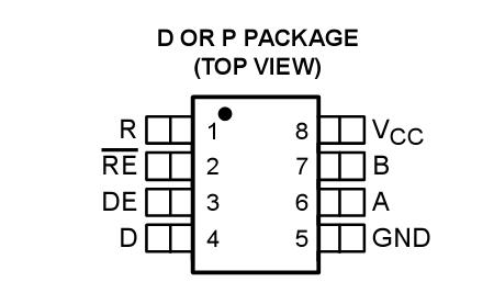
Digital Motor ControlPinout Specifications
|
|
SN65HVD05, SN65HVD06, SN65HVD07
SN75HVD05, SN75HVD06, SN75HVD07 |
|
Supply voltage range, V CC |
0.3 V to 6 V |
|
Voltage range at A or B |
9 V to 14 V |
|
Input voltage range at D, DE, R or RE |
0.5 V to VCC + 0.5 V |
|
Voltage input range, transient pulse, A and B, through 100 ? (see Figure 11) |
50 V to 50 V |
|
Electrostatic discharge |
Humanbodymodel(3) |
A,B,andGND |
16 kV |
|
Charged-devicemodel(4)
|
Allpins |
4 kV |
|
All pins |
1 kV |
|
Continuous total power dissipation |
See Dissipation Rating Table |
|
Storage temperature range, Tstg |
65 to 150 |
|
Leadtemperature 1,6 mm (1/16 inch) from case for 10 seconds |
260 |
DescriptionThe SN65HVD05, SN75HVD05, SN65HVD06,SN75HVD06, SN65HVD07, and SN75HVD07 combinea 3-state differential line driver and differential linereceiver. SN65HVD05, SN75HVD05, SN65HVD06,SN75HVD06, SN65HVD07, and SN75HVD07 are designed for balanced datatransmission and interoperate with ANSITIA/EIA-485-A and ISO 8482E standard-compliantdevices. The driver is designed to provide a differentialoutput voltage greater than that required by thesestandards for increased noise margin. The drivers andreceivers have active-high and active-low enablesrespectively, SN65HVD05, SN75HVD05, SN65HVD06,SN75HVD06, SN65HVD07, and SN75HVD07 can be externally connectedtogether to function as direction control.
The driver differential outputs and receiver differential inputs of SN65HVD05, SN75HVD05, SN65HVD06,SN75HVD06, SN65HVD07, and SN75HVD07 connect internally to form a differential input/output (I/O) bus port that is designed to offer minimumloading to the bus whenever the driver is disabled or notpowered. SN65HVD05, SN75HVD05, SN65HVD06,SN75HVD06, SN65HVD07, and SN75HVD07 feature wide positive andnegative common-mode voltage ranges, making themsuitable for party-line applications.

 SN65HVD05 Data Sheet


