Features: ` Controlled Baseline
One Assembly/Test Site, One Fabrication Site
` Extended Temperature Performance of
40°C to 125°C
` Enhanced Diminishing Manufacturing Sources (DMS) Support
` Enhanced Product Change Notification
` Qualification Pedigree†
`High-Speed Low-Power LinBiCMOSTM Circuitry Designed for Signaling Rates‡ Up to 30 Mbps
` Bus-Pin ESD Protection Exceeds 12-kV HBM
` Compatible With ANSI Standard TIA/EIA-485-A and ISO 8482:1987(E)
` Low Skew
` Designed for Multipoint Transmission on Long Bus Lines in Noisy Environments
` Low Disabled Supply Current Requirements . . . 700 A Maximum
` Common Mode Voltage Range of 7 V to 12 V
` Thermal-Shutdown Protection
` Driver Positive and Negative Current Limiting
` Open-Circuit Fail-Safe Receiver Design
` Receiver Input Sensitivity . . . ±200 mV Max
` Receiver Input Hysteresis . . . 50 mV Typ
` Glitch-Free Power-Up and Power-Down Protection
† Component qualification in accordance with JEDEC and industry standards to ensure reliable operation over an extended temperature range. This includes, but is not limited to, Highly Accelerated Stress Test (HAST) or biased 85/85, temperature cycle, autoclave or unbiased HAST, electromigration, bond intermetallic life, and mold compound life. Such qualification testing should not be viewed as justifying use of this component beyond specified performance and environmental limits.
‡ Signaling rate by TIA/EIA-485-A definition restrict transition times to 30% of the bit length, and much higher signaling rates may be achieved without this requirement as displayed in the TYPICAL CHARACTERISTICS of this device.
Pinout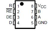 Specifications
Supply voltage, VCC (see Note 1) . . . . . . . . . . . . . . . . . . . . . . . . . . . . . . . . . . . . . . . . . 0.3 V to 6 V
Voltage range at any bus terminal (A or B) . . . . . . . . . . . . . . . . . . . . . . . . . . . . . . . . . . 10 V to 15 V
Input voltage, VI (D, DE, R, or RE) . . . . . . . . . . . . . . . . . . . . . . . . . . . . . . . . .. . 0.3 V to VCC + 0.5 V
Electrostatic discharge:Bus terminals and GND, Class 3, A: (see Note 2) . . . . . . . . . . . . . . . . . . 12 kV
Bus terminals and GND, Class 3, B: (see Note 2) . . . . . . . . . . . . . . . . . 400 V
All terminals, Class 3, A: . . . . . . . . . . . . . . . . . . . . . . . . . . . . . . . . . . . . . 4 kV
All terminals, Class 3, B: . . . . . . . . . . . . . . . . . . . . . . . . . . . . . . . . . . . . 400 V
Continuous total power dissipation (see Note 3) . . . . . . . . . . . . . . . . . . See Dissipation Rating Table
Storage temperature range, Tstg . . . . . . . . . . . . . . . . . . . . . . . . . . . . . . . . . . . . . . 65°C to 150°C
Lead temperature 1,6 mm (1/16 inch) from case for 10 seconds . . . . . . . . . . . . . . . . . . . . . . . 260°C
† Stresses beyond those listed under "absolute maximum ratings" may cause permanent damage to the device. These are stress ratings only, and functional operation of the device at these or any other conditions beyond those indicated under "recommended operating conditions" is not implied. Exposure to absolute-maximum-rated conditions for extended periods may affect device reliability.
NOTES: 1. All voltage values, except differential I/O bus voltage, are with respect to network ground terminal.
2. The maximum operating junction temperature is internally limited. Use the dissipation rating table to operate below this temperature.
3. Tested in accordance with MILSTD883C, Method 3015.7
DescriptionThe SN65LBC176A-EP differential bus transceiver is a monolithic, integrated circuits designed for bidirectional data communication on multipoint bus-transmission lines. The SN65LBC176A-EP is designed for balanced transmission lines and is compatible with ANSI standard TIA/EIA-485-A and ISO 8482. The SN65LBC176A-EP offers improved switching performance over its predecessors without sacrificing significantly more power.
The SN65LBC176A-EP combines a 3-state, differential line driver and a differential input line receiver, both of which operate from a single 5-V power supply. The driver and receiver have active-high and active-low enables, respectively, SN65LBC176A-EP can externally connect together to function as a direction control. The driver differential outputs and the receiver differential inputs connect internally to form a differential input/output (I/O) bus port that is designed to offer minimum loading to the bus whenever the driver is disabled or VCC = 0. This port features wide positive and negative common-mode voltage ranges, making the SN65LBC176A-EP suitable for party-line applications. Low device supply current can be achieved by disabling the driver and the receiver.

 SN65LBC176A-EP Data Sheet


