SN65LBC184

Features: Integrated Transient Voltage SuppressionESD Protection for Bus Terminals: ±15 kV Human Body Model ±8 kV IEC1000-4-2, Contact Discharge ±15 kV IEC1000-4-2, Air-Gap DischargeCircuit Damage Protection of 400 W Peak(Typical)Controlled Driver Output-Voltage SlewRates Allows Longer Cable St...

product image

SN65LBC184 Picture
SeekIC No. : 004497425 Detail

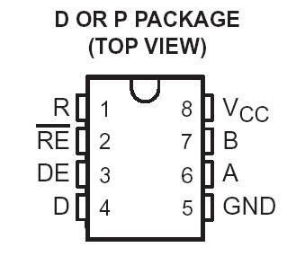
SN65LBC184: Features: Integrated Transient Voltage SuppressionESD Protection for Bus Terminals: ±15 kV Human Body Model ±8 kV IEC1000-4-2, Contact Discharge ±15 kV IEC1000-4-2, Air-Gap DischargeCircuit Damag...

floor Price/Ceiling Price

Part Number:
SN65LBC184
Supply Ability:
5000

Price Break

  • Qty
  • 1~5000
  • Unit Price
  • Negotiable
  • Processing time
  • 15 Days
Total Cost: $ 0.00

SeekIC Buyer Protection PLUS - newly updated for 2013!

  • Escrow Protection.
  • Guaranteed refunds.
  • Secure payments.
  • Learn more >>

Month Sales

268 Transactions

Rating

evaluate  (4.8 stars)

Upload time: 2024/5/7

Payment Methods

All payment methods are secure and covered by SeekIC Buyer Protection PLUS.

Notice: When you place an order, your payment is made to SeekIC and not to your seller. SeekIC only pays the seller after confirming you have received your order. We will also never share your payment details with your seller.
Product Details

Description


Features:

Integrated Transient Voltage Suppression
ESD Protection for Bus Terminals:
   ±15 kV Human Body Model
   ±8 kV IEC1000-4-2, Contact Discharge
   ±15 kV IEC1000-4-2, Air-Gap Discharge
Circuit Damage Protection of 400 W Peak(Typical)
Controlled Driver Output-Voltage SlewRates Allows Longer Cable Stub Lengths
250-kbits/s niElectrically NoisyEnvironments
Open-Circuit Fail-Safe Receiver Design
1/2 Unit Load Allows for 64 DevicesConnected on Bus
TherShutdown Protection
Power-Up/-Down Glitch Protectionmal
Each Transceiver Meets or Exceeds theRequirements of EIA RS-485 and ISO/IEC8482:1993(E) Standards
Low Disabled Supply Current 300 uA Max
Pin Compatible with SN75176


Pinout

  Connection Diagram


Specifications

Supply voltage, VCC (see Note 1) . . . . . . . . . . . . .  . . . . . . . . . . . . . . . . . . . . . . .0.5 V to 7 V
Continuous voltage range at any bus terminal . . . . . . . . . . . . . . . . . . . . . . . . . .15 V to 15 V
Data input/output voltage . . . . . . . . . . . . . . . . . . . . . . . . . . . . . .  . . . . . . . . . . . .0.3 V to 7 V
Electrostatic discharge:
                                     All Terminals (Class 3 A) (see Note 3)  . . . . . . . . . . . . . . . . . . . . . .8 kV
                                     All Terminals (Class 3 B) (see Note 3)  . . . . . . . . . . . . . . . . . . . .1200 V
Continuous total power dissipation (see Note 2)  . . .  . . . . . . . . . . . . . . . . . .Internally Limited
Operating free-air temperature range, TA:SN65LBC184  . . . . . . . . . . . . . . . . . . .40 to 85
                                                                  SN75LBC184  . . . . . . . . . . . . . .  . . . . . . . .0to 70
Storage temperature range, Tstg  . . . . . . . . . . . . . . . . . . . . . . . . . . . . . . . . . . . . 65to 150
Lead temperature 1,6 mm (1/16 inch) from case for 10 seconds  . . . . . . . . . . . . . . . . . . . .260


Description

The SN75LBC184 and SN65LBC184 are differentialdata line transceivers in the trade-standardfootprint of theSN75176 with built-in protectionagainst high-energy noise transients. SN75LBC184 and SN65LBC184 feature provides a substantial increase in reliability forbetter immunity to noise transients coupled to thedata cable over most existing devices. Use ofthese circuits provides a reliable low-costdirect-coupled (with no isolation transformer) dataline interface without requiring any externalcomponents.

The SN75LBC184 and SN65LBC184 can withstandovervoltage transients of 400 W peak(typical). The conventional combination wavecalled out in CEI IEC 1000-4-5 simulates theovervoltage transient and models a unidirectional surge caused by overvoltages from switching andsecondary lightning transients.

A biexponential function of SN75LBC184 and SN65LBC184 defined by separate rise and fall times for voltage and current simulates thecombination wave. The standard 1.2 ms/50 ms combination waveform is shown in Figure 1 and in the testdescription in Figure 9.

The SN75LBC184 and SN65LBC184 also includes additional desirable features for party-line data buses in electrically noisy environmen tapplications including industrial process control. The differential-driver design incorporates slew-rate-controlled outputs sufficient to transmit data up to 250 kbits/s. Slew-rate control allows longer unterminated cable runs andlonger stub lengths from the main backbone than possible with uncontrolled and faster voltage transitions. Aunique receiver design provides a fail-safe output of a high level when the inputs are left floating (open circuit).The SN75LBC184 and SN65LBC184 receiver also includes a high input resistance equivalent to one-half unitload allowing connection of up to 64 similar devices on the bus.

The SN75LBC184 is characterized for operation from 0 to 70. The SN65LBC184 is characterized from40 to 85.


Customers Who Bought This Item Also Bought

Margin,quality,low-cost products with low minimum orders. Secure your online payments with SeekIC Buyer Protection.
Discrete Semiconductor Products
Transformers
Cable Assemblies
Batteries, Chargers, Holders
Circuit Protection
View more