Features: ` High Speed 2x2 LVPECL Crosspoint Switch
` LVDS Crosspoint Switch Available in SN65LVCP22
` 50 ps (Typ), of Peak-to-Peak Jitter With PRBS = 2231 Pattern
` Output (Channel-to-Channel) Skew Is 10 ps (Typ), 50 ps (Max)
` Configurable as 2:1 Mux, 1:2 Demux, Repeater or 1:2 Signal Splitter
` Inputs Accept LVDS, LVPECL, and CML Signals
` Fast Switch Time of 1.7 ns (Typ)
` Fast Propagation Delay of 0.75 ns (Typ)
` 16 lead SOIC and TSSOP Packages
` Operating Temperature: 40°C to 85°CApplication· Gigabit Ethernet Redundant Transmission Paths
· Gigabit Interface Converters (GBICs)
· Fibre Channel Redundant Transmission Paths
· HDTV Video Routing
· Base Stations
· Protection Switching for Serial Backplanes
· Network Switches/Routers
· Optical Networking Line Cards/Switches
· Clock DistributionPinout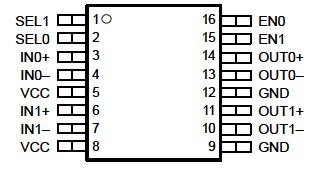 Specificationsover operating free-air temperature range unless otherwise noted(1)
| |
UNITS |
| Supply voltage(2) range, VCC |
0.5 V to 4 V |
| CMOS/TTL input voltage (ENO, EN1, SEL0, SEL1) |
0.5 V to 4 V |
| Receiver Input voltage (IN+, IN) |
0.7 V to 4.3 V |
| LVPECL driver output voltage (OUT+, OUT) |
0.5 V to 4 V |
| Output current |
Continuous |
50 mA |
| Surge |
100 mA |
| Storage temperature range |
65°C to 125°C |
| Lead temperature 1,6 mm (1/16 inch) from case for 10 seconds |
235°C |
| Continuous power dissipation |
See Dissipation Rating Table |
| Electrostatic discharge |
Human body model(3) |
All pins |
±5 kV |
| Charged-device mode(4) |
All pins |
±500 V |
(1) Stresses beyond those listed under "absolute maximum ratings" may cause permanent damage to the device. These are stress ratings only, and functional operation of the device at these or any other conditions beyond those indicated under "recommended operating conditions" is not implied. Exposure to absolute-maximum-rated conditions for extended periods may affect device reliability.
(2) All voltage values, except differential I/O bus voltages, are with respect to network ground terminals.
(3) Tested in accordance with JEDEC Standard 22, Test Method A114-A.
(4) Tested in accordance with JEDEC Standard 22, Test Method C101.
DescriptionThe SN65LVCP23 is a 2x2 LVPECL crosspoint switch. The dual channels incorporate wide common-mode (0 V to 4 V) receivers, allowing for the receipt of LVDS, LVPECL, and CML signals. The dual outputs are LVPECL drivers to provide high-speed operation. The SN65LVCP23 provides a single device supporting 2:2 buffering (repeating), 1:2 splitting, 2:1 multiplexing, 2x2 switching, and LVDS/CML to LVPECL level translation on each channel. The flexible operation of the SN65LVCP23 provides a single device to support the redundant serial bus transmission needs (working and protection switching cards) of fault-tolerant switch systems found in optical networking, wireless infrastructure, and data communications systems. TI offers an additional gigibit repeater/ translator in the SN65LVDS101.
The SN65LVCP23 uses a fully differential data path to ensure low-noise generation, fast switching times, low pulse width distortion, and low jitter. Output channel-to-channel skew is less than 10 ps (typ) and 50 ps (max) to ensure accurate alignment of outputs in all applications. Both SOIC and TSSOP package options are available.

 SN65LVCP23 Data Sheet


