Features: ` Qualification in Accordance With AEC-Q100†
` Qualified for Automotive Applications
` Customer-Specific Configuration Control Can Be Supported Along With Major-Change Approval
` ESD Protection Exceeds 2000 V Per MIL-STD-883, Method 3015; Exceeds 200 V Using Machine Model (C = 200 pF, R = 0)
` Low-Voltage Differential 50- Line Drivers and Receivers
` Signaling Rates up to 500 Mbps
` Bus-Terminal ESD Exceeds 12 kV
` Operates From a Single 3.3 V Supply
` Low-Voltage Differential Signaling With Typical Output Voltages of 340 mV With a 50- Load
` Valid Output With as Little as 50-mV Input Voltage Difference
` Propagation Delay Times
Driver: 1.7 ns Typ
Receiver: 3.7 ns Typ
` Power Dissipation at 200 MHz
Driver: 50 mW Typical
Receiver: 60 mW Typical
` LVTTL Input Levels Are 5 V Tolerant
` Driver Is High Impedance When Disabled or With VCC < 1.5 V
` Receiver Has Open-Circuit Fail Safe
† Contact factory for details. Q100 qualification data available on request.Pinout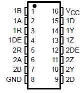
SpecificationsSupply voltage range, VCC (see Note 1) . . . . . . . . . . . . . . . . . . . . . . . . . . . . . . . . . . .. . . . 0.5 V to 4 V
Voltage range (D, R, DE, RE) . . . . . . . . . . . . . . . . . . . . . . . . . . . . . . . . . . . . . . . . .. . . . . . . 0.5 V to 6 V
Voltage range (Y, Z, A, and B) . . . . . . . . . . . . . . . . . . . . . . . . . . . . . . . . . . . . .. . . . . . . . . . 0.5 V to 4 V
Electrostatic discharge: Y, Z, A, B , and GND (see Note 2) . . . . . . . . . . . . . .. . CLass 3, A:12 kV, B:600 V
All . . . . . . . . . . . . . . . . . . . . . . . . . . . . . . . . . . . . . . . . . Class 3, A:7 kV, B:500 V
Continuous power dissipation . . . . . . . . . . . . . . . . . . . . . . . . . . . . . . . . . . . . see dissipation rating table
Storage temperature range . . . . . . . . . . . . . . . . . . . . . . . . . . . . . . . . . . . . . . . . . . .. . 65°C to 150°C
Lead temperature 1,6 mm (1/16 inch) from case for 10 seconds . . . . . . . . . . . . . . . . .. . . . . . . . . 250°C
† Stresses beyond those listed under "absolute maximum ratings" may cause permanent damage to the device. These are stress ratings only, and functional operation of the device at these or any other conditions beyond those indicated under "recommended operating conditions" is not implied. Exposure to absolute-maximum-rated conditions for extended periods may affect device reliability.
NOTES: 1. All voltage values, except differential I/O bus voltages, are with respect to network ground terminal.
2. Tested in accordance with MIL-STD-883C Method 3015.7.
DescriptionThe SN65LVDM050, and SN65LVDM051 are differential line drivers and receivers that use low-voltage differential signaling (LVDS) to achieve signaling rates as high as 500 Mbps (per TIA/EIA-644 definition). These circuits are similar to TIA/EIA-644 standard compliant devices (SN65LVDS) counterparts, except that the output current of the drivers is doubled. This modification provides a minimum differential output voltage magnitude of 247 mV across a 50- load simulating two transmission lines in parallel. SN65LVDM050, and SN65LVDM051 allows having data buses with more than one driver or with two line termination resistors. The receivers detect a voltage difference of 50 mV with up to 1 V of ground potential difference between a transmitter and receiver.
The intended application of SN65LVDM050, and SN65LVDM051 and signaling techniques is point-to-point and multipoint, baseband data transmission over a controlled impedance media of approximately 100 of characteristic impedance. The transmission media of SN65LVDM050, and SN65LVDM051 may be printed-circuit board traces, backplanes, or cables.

 SN65LVDM051-Q1 Data Sheet


