Features: >400 Mbps (200 MHz) Signaling Rates
Flow-Through Pinout Simplifies PCB Layout
50 ps Channel-to-Channel Skew (Typ)
200 ps Differential Skew (Typ)
Propagation Delay Times 2.7 ns (Typ)
3.3-V Power Supply Design
High Impedance LVDS Inputs on Power Down
Low-Power Dissipation (40 mW at 3.3 V Static)
Accepts Small Swing (350 mV) Differential Signal Levels
Supports Open, Short, and Terminated Input Fail-Safe
Industrial Operating Temperature Range (40°C to 85°C)
Conforms to TIA/EIA-644 LVDS Standard
Available in SOIC and TSSOP Packages
Pin-Compatible With DS90LV048A From National
ApplicationOne of the most common problems with differential signaling applications is how the system responds when no differential voltage is present on the signal pair. The LVDS receiver is like most differential line receivers, in that its output logic state can be indeterminate when the differential input voltage is between 100 mV and 100 mV and within its recommended input common-mode voltage range. TI's LVDS receiver is different in how it handles the open-input circuit situation, however.
Open-circuit means that there is little or no input current to the receiver from the data line itself. This could be when the driver is in a high-impedance state or the cable is disconnected. When this occurs, the LVDS receiver will pull each line of the signal pair to near VCC through 300-k resistors as shown in Figure 10. The fail-safe feature uses an AND gate with input voltage thresholds at about 2.3 V to detect this condition and force the output to a high-level regardless of the differential input voltage.
It is only under these conditions that the output of the receiver will be valid with less than a 100-mV differential input voltage magnitude. The presence of the termination resistor, Rt, does not affect the fail-safe function as long as it is connected as shown in the figure. Other termination circuits may allow a dc current to ground that could defeat the pullup currents from the receiver and the fail-safe feature.
Pinout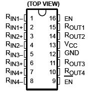 Specifications
Supply voltage range (VCC) . . . . . . . . . . . . . . . . . . . . . . . . . . . . . . . . . . . . . . . . . . . . . . . . . . . . . . . . . .0.3 V to 4 V
Input voltage range, VI(RIN+, RIN) . . . . . . . . . . . . . . . . . . . . . . . . . . . . . . . . . . . . . . . . . . . . . . . . . . . 0.3 V to 4 V
Enable input voltage (EN, EN ) . . . . . . . . . . . . . . . . . . . . . . . . . . . . . . . . . . . . . . . . . . . . . . ....0.3 V to (VCC +0.3 V)
Output voltage, VO(ROUT) . . . . . . . . . . . . . . . . . . . . . . . . . . . . . . . . . . . . . . . . . . . . . . . . . . ...0.3 V to (VCC +0.3 V)
Bus-pin (RIN+, RIN) Electrostatic discharge (see Note 2) . . . . . . . . . . . . . . . . . . . . . . . . . . . . . . . . . . . . ......> 10 kV
Continuous power dissipation . . . . . . . . . . . . . . . . . . . . . . . . . . . . . . . . . . . . . . . . .... ...See Dissipation Rating Table
Storage temperature range . . . . . . . . . . . . . . . . . . . . . . . . . . . . . . . . . . . . . . . . . . . . . . . . . . . . . . 65°C to 150°C
Lead temperature 1,6 mm (1/16 inch) from case for 10 seconds . . . . . . . . . . . . . . . . . . . . . . . . . . . . . . . .......260°C
DescriptionThe SN65LVDS048A is a quad differential line receiver that implements the electrical characteristics of low-voltage differential signaling (LVDS). This signaling technique lowers the output voltage levels of 5-V differential standard levels (such as EIA/TIA-422B) to reduce the power, increase the switching speeds, and allow operation with a 3.3-V supply rail. Any of the quad differential receivers will provide a valid logical output state with a ±100-mV differential input voltage within the input common-mode voltage range. The input common-mode voltage range of SN65LVDS048A allows 1 V of ground potential difference between two LVDS nodes.
The intended application of SN65LVDS048A and signaling technique is for point-to-point baseband data transmission over controlled impedance media of approximately 100 . The transmission media may be printed-circuit board traces, backplanes, or cables. The ultimate rate and distance of data SN65LVDS048A transfer is dependent upon the attenuation characteristics of the media, the noise coupling to the environment, and other system characteristics.
The SN65LVDS048A is characterized for operation from 40°C to 85°C.

 SN65LVDS048A Data Sheet


