ApplicationThe SN65LVDS108 device solves several problems common to the distribution of timing critical clock and data signals. These problems include:
·Excessive skew between the signal paths
·Noise pickup over long signaling paths
·High power consumption
·Control of which signal paths are enabled or disabled
·Elimination of radiation from unterminated lines
Buffering and splitting the signal on the same silicon die minimizes corruption of the timing relation between the copies of the signal. Buffering and splitting the signal in separate devices will introduce considerably higher levels of uncontrolled timing skew between the signals. Higher speed operation and more timing tolerance for other components of the system is enabled by the tighter system timing budgets provided by the single die
implementations of the SN65LVDS108.
The use of LVDS signaling technology for both the inputs and the outputs provides superior common-mode and noise tolerance compared to single-ended I/O technologies. This is particularly important because the signals that are being distributed must be transmitted over longer distances, and at higher rates, than can be accommodated with single-ended I/Os. In addition, LVDS consumes considerably less power than other high-performance differential signaling schemes.
The enable inputs provided for each output may be used to turn on or off any of the paths. This function is required to prevent radiation of signals from the unterminated signal lines on open connectors when boards or devices are being swapped in the end equipment. The individual channel enables are also required if redundant paths are being utilized for reliability reasons.
The following diagram shows how an input signal is being identically repeated out two of the available outputs.A third output is shown in the disabled state.
Pinout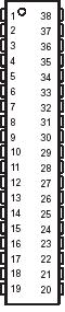 SpecificationsSupply voltage range, VCC (see Note 1) . . . . . . . . . . . . . . . . . . . . .. . . . . . . . . . . . . . .0.5 V to 4 V
Input voltage range, Enable inputs . . . . . . . . . . . . . . . . . . . . . . . . . . . . . . . . . . . . . . .0.5 V to 6 V
A, B, Y or Z . . . . . . . . . . . . . . . . . . . . . . . . . . . . . . . . . . . . . . . .. .0.5 V to 4 V
Electrostatic discharge, Y, Z, and GND (see Note 2) . . . . . . . . . . . . . .. . . .Class 3, A:12 kV, B: 500 V
All pins . . . . . . . . . . . . . . .. . . . . . . . . . . . . . . . . . ..Class 3, A: 4 kV, B: 400 V
Continuous power dissipation . . . . . . . . . . . . . . . . . . . . . . . . . . . . . . . .See Dissipation Rating Table
Storage temperature range . . . . . . . . . . . . . . . . . . . . . . . . . . . . . . . . . . . . . . . . .65°C to 150°C
Lead temperature 1,6 mm (1/16 inch) from case for 10 seconds . . . . . . . .. . . . . . . . . . . . . . .260°CDescriptionThe SN65LVDS108 is configured as one differential line receiver connected to eight differential line drivers.Individual output enables are provided for each output and an additional enable is provided for all outputs.
The line receivers and line drivers implement the electrical characteristics of low-voltage differential signaling SN65LVDS108 (LVDS). LVDS, as specified in EIA/TIA-644, is a data signaling technique that offers low power, low noise emission, high noise immunity, and high switching speeds. SN65LVDS108 can be used to transmit data at speeds up to at least 622 Mbps and over relatively long distances. (Note: The ultimate rate and distance of data transfer is dependent upon the attenuation characteristics of the media, the noise coupling to the environment, and other system characteristics.)
The intended application of SN65LVDS108, and the LVDS signaling technique, is for point-to-point or point-to-multipoint (distributed simplex) baseband data transmission on controlled impedance media of approximately 100 W. The transmission media may be printed-circuit board traces, backplanes, or cables. The large number of SN65LVDS108 integrated into the same silicon substrate, along with the low pulse skew of balanced signaling, provides extremely precise timing alignment of the signals being repeated from the inputs. This is particularly advantageous for implementing system clock or data distribution trees.
The SN65LVDS108 is characterized for operation from 40°C to 85°C.

 SN65LVDS108 Data Sheet


