Features: · A Member of the MuxItTM Serializer- Deserializer Building-Block Chip Family
· Pin Selectable Frequency Multiplier Ratios Between 4 and 40
· Input Clock Frequencies From 5 to 50 MHz
· Multiplied Clock Frequencies up to 400 MHz
· Internal Loop Filters and Low PLL-Jitter of 20 ps RMS Typical at 200 MHz
· LVDS Compatible Differential Inputs and Outputs Meet or Exceed the Requirements of ANSI EIA/TIA-644-A
· LVTTL Compatible Inputs Are 5 V Tolerant
· LVDS Inputs and Outputs ESD Protection Exceeds 12 kV HBM
· Operates From a Single 3.3 V Supply
· Packaged in 28-Pin Thin Shrink Small-Outline Package With 26 mil Terminal PitchPinout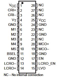 Specifications
Supply voltage range, VCC (see Note 1) . . . . . . . . . . . . . . . . . . . . . . . . . . . . . . . . . . . . . . . . . . 0.5 V to 4 V
Voltage range: EN, BSEL, LCRO_EN, or M1M5 inputs . . . . . . . . . . . . . . . . . . . . . . . . . . . . . . . 0.5 V to 6 V
CRI input . . . . . . . . . . . . . . . . . . . . . . . . . . . . . . . . . . . . . . . . . . . . . . . . . . . . . . 0.5 V to 4 V
LCRO±, MCO± outputs . . . . . . . . . . . . . . . . . . . . . . . . . . . . . . . . . . . . . . . . . . .0.5 V to 4 V
Electrostatic discharge: Human body model (CRI±, LCRO±, MCO±,and GND (see Note 2) . . . . . . . . ±12 kV
All pins . . . . . . . . . . . . . . . . . . . . . . . . . . . . . . . . . . . . . . . . . . . . . . . . . . . . . . . ±2 kV
Charged-device model (all pins) (see Note 3) . . . . . . . . . . . . . . . . . . . . . . .. . ±500 V
Continuous total power dissipation . . . . . . . . . . . . . . . . . . . . . . . . . . . . . . . . . . See Dissipation Rating Table
Storage temperature range, Tstg . . . . . . . . . . . . . . . . . . . . . . . . . . . . . . . . . . . . . . . . .. . . . 65C to 150
Lead temperature 1,6 mm (1/16 inch) from case for 10 seconds . . . . . . . . . . . . . . . . . . . . . . . . . . . . . . 260
† Stresses beyond those listed under "absolute maximum ratings" may cause permanent damage to the device. These are stress ratings only, and functional operation of the device at these or any other conditions beyond those indicated under "recommended operating conditions" is not implied. Exposure to absolute-maximum-rated conditions for extended periods may affect device reliability.
NOTES: 1. All voltages, except differential I/O bus voltages, are with respect to the network ground terminal.
2. Tested in accordance with JEDEC Standard 22, Test method A114-B.
3. Tested in accordance with JEDEC Standard 22, Test method C101.
DescriptionThe MuxIt SN65LVDS150 is a family of general-purpose, multiple-chip building blocks for implementing parallel data serializers and deserializers. The system allows for wide parallel data to be transmitted through a reduced number of differential transmission lines over distances greater, SN65LVDS150 can be achieved with a single-ended (e.g., LVTTL or LVCMOS) data interface. The number of bits multiplexed per transmission line is user selectable, allowing for higher transmission efficiencies than with other existing fixed ratio solutions. Muxlt SN65LVDS150 utilizes the LVDS (TIA/EIA-644) low voltage differential signaling technology for communications between the data source and data destination.
The MuxIt family initially includes three devices supporting simplex communications; The SN65LVDS150 Phase Locked Loop-Frequency Multiplier, The SN65LVDS151 Serializer-Transmitter, and The SN65LVDS152 Receiver-Deserializer.
The SN65LVDS150 is a PLL based frequency multiplier designed for use with the other members of the MuxIt family of serializers and deserializers. The frequency multiplication ratio is pin selectable over a wide range of values from 4 through 40 to accommodate a broad spectrum of user needs. No external filter components are needed. A PLL SN65LVDS150 lock indicator output is available which may be used to enable link data transfers.

 SN65LVDS150 Data Sheet


