SN65LVDS307

Features: ` FlatLink™ 3G Serial-Interface Technology` Compatible With FlatLink™3G Receivers Such as SN65LVDS308` Input Supports Video Interfaces up to 24-Bit RGB Data and 3 Control Bits Received Over Two Differential Data Lines` SubLVDS Differential Voltage Levels` Up to 810-Mbps Data ...

product image

SN65LVDS307 Picture
SeekIC No. : 004497482 Detail

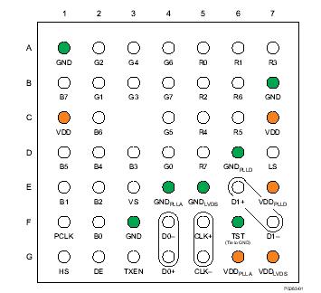
SN65LVDS307: Features: ` FlatLink™ 3G Serial-Interface Technology` Compatible With FlatLink™3G Receivers Such as SN65LVDS308` Input Supports Video Interfaces up to 24-Bit RGB Data and 3 Control Bits ...

floor Price/Ceiling Price

Part Number:
SN65LVDS307
Supply Ability:
5000

Price Break

  • Qty
  • 1~5000
  • Unit Price
  • Negotiable
  • Processing time
  • 15 Days
Total Cost: $ 0.00

SeekIC Buyer Protection PLUS - newly updated for 2013!

  • Escrow Protection.
  • Guaranteed refunds.
  • Secure payments.
  • Learn more >>

Month Sales

268 Transactions

Rating

evaluate  (4.8 stars)

Upload time: 2025/12/24

Payment Methods

All payment methods are secure and covered by SeekIC Buyer Protection PLUS.

Notice: When you place an order, your payment is made to SeekIC and not to your seller. SeekIC only pays the seller after confirming you have received your order. We will also never share your payment details with your seller.
Product Details

Description


Features:

` FlatLink™ 3G Serial-Interface Technology
` Compatible With FlatLink™3G Receivers Such as SN65LVDS308
` Input Supports Video Interfaces up to 24-Bit RGB Data and 3 Control Bits Received Over Two Differential Data Lines
` SubLVDS Differential Voltage Levels
` Up to 810-Mbps Data Throughput
` Three Operating Modes to Conserve Power
    Active-Mode QVGA, 60 fps, 17.4 mW (typ)
    Active-Mode VGA, 60 fps, 28.8 mW (typ)
    Shutdown Mode » 0.9 mW (typ)
    Standby Mode » 0.9 mW (typ)
` 1.8-V Supply Voltage
` ESD Rating > 3 kV (HBM)
` Pixel Clock Range of 4 MHz30 MHz
` Failsafe on All CMOS Inputs
` 4-mm ´ 4-mm MicroStar Junior™mBGA® Package With 0,5-mm Ball Pitch
` Very Low EMI


Application

· Host-Controller to Display-Module Interface
· Mobile Phones and Smart Phones
· Portable Multimedia Players


Pinout

  Connection Diagram


Specifications

  VALUE UNIT
Supply voltage range, VDD(2), VDDPLLA, VDDPLLD, VDDLVDS 0.3 to 2.175 V
Voltage range at any input
or output terminal
When VDDx > 0 V 0.5 to 2.175 V
When VDDx  0 V 0.5 to VDD + 2.175 V
Electrostatic discharge Human-body model(3) (all terminals) ±3 kV
Charged-device model(4) (all terminals) ±500 V
Machine model(5) (all terminals) ±200
Continuous power dissipation See Dissipation Ratings table


(1) Stresses beyond those listed under absolute maximum ratings may cause permanent damage to the device. These are stress ratings only and functional operation of the device at these or any other conditions beyond those indicated under recommended operating conditions is not implied. Exposure to absolute maximum-rated conditions for extended periods may affect device reliability.
(2) All voltage values are with respect to the GND terminals.
(3) In accordance with JEDEC Standard 22, Test Method A114-A.
(4) In accordance with JEDEC Standard 22, Test Method C101.
(5) In accordance with JEDEC Standard 22, Test Method A115-A


Description

The SN65LVDS307 serializer device converts 27 parallel data inputs to one or two sub-low-voltage differential signaling (SubLVDS) serial outputs. SN65LVDS307 loads a shift register with 24 pixel bits and 3 control bits from the parallel CMOS input interface. In addition to the 27 data bits, the device adds a parity bit and two reserved bits into a 30-bit data word. Each word is latched into the device by the pixel clock (PCLK). The parity bit (odd parity) allows a receiver to detect single bit errors. The serial shift register SN65LVDS307 is uploaded at 30 or 15 times the pixel-clock data rate, depending on the number of serial links used. A copy of the pixel clock is output on a separate differential output.

FPC cabling typically interconnects the SN65LVDS307 with the display. Compared to parallel signaling, the SN65LVDS307 outputs significantly reduce the EMI of the interconnect by over 20 dB.

The SN65LVDS307 supports three power modes (shutdown, standby, and active) to conserve power. When transmitting, the PLL locks to the incoming pixel clock, PCLK, and generates an internal high-speed clock at the line rate of the data lines. The parallel data SN65LVDS307 are latched on the rising or falling edge of PCLK, as selected by the external control signal CPOL. The serialized data is presented on the serial outputs D0 and D1, together with a recreated PCLK that is generated from the internal high-speed clock and output on CLK. If PCLK stops, the device enters a standby mode to conserve power.


Customers Who Bought This Item Also Bought

Margin,quality,low-cost products with low minimum orders. Secure your online payments with SeekIC Buyer Protection.
Industrial Controls, Meters
Sensors, Transducers
Resistors
Cables, Wires
Computers, Office - Components, Accessories
View more