Features: · Designed for Signaling Rates (1) ³ 2 Gbps
· Total Jitter < 65 ps
· Low-Power Alternative for the MC100EP16
· Low 100 ps (Max) Part-To-Part Skew
· 25 mV of Receiver Input Threshold Hysteresis Over 0-V to 4-V Common-Mode Range
· Inputs Electrically Compatible With LVPECL,CML, and LVDS Signal Levels
· 3.3-V Supply Operation
· LVDT Integrates 110-W Terminating Resistor
· Offered in SOIC and MSOPApplication· 622 MHz Central Office Clock Distribution
· High-Speed Network Routing
· Wireless Basestations
· Low Jitter Clock Repeater
· Serdes LVPECL Output to FPGA LVDS Input TranslatorPinout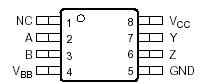 Specifications
|
UNIT |
| VCC Supply voltage(2) |
0.5 V to 4 V |
| IBB VBB Output current |
±0.5 mA |
| VI |
Voltage range, (A, B, Y, Z) |
0 V to 4.3 V |
| VO |
| VID Differential voltage, |VA VB| ('LVDT100 and 'LVDT101 only) |
1 V |
|
ESD |
Human Body Model(3) |
A, B, Y, Z, and GND |
±5 kV |
| All pins |
±2 kV |
| Charged-Device Model(4) |
All pins |
±1500 V |
|
PD Continuous power dissipation |
See Dissipation Rating Table |
(1) Stresses beyond those listed under absolute maximum ratings may cause permanent damage to the device. These are stress ratings only, and functional operation of the device at these or any other conditions beyond those indicated under recommended operating conditions is not implied. Exposure to absolute-maximum-rated conditions for extended periods may affect device reliability.
(2) All voltage values, except differential I/O bus voltages, are with respect to network ground terminal.
(3) Tested in accordance with JEDEC Standard 22, Test Method A114-A.7.
(4) Tested in accordance with JEDEC Standard 22, Test Method C101.
DescriptionThe SN65LVDS100, SN65LVDT100, SN65LVDS101,and SN65LVDT101 are a high-speed differential re-ceiver and driver connected as a repeater. The receiver accepts low-voltage differential signaling (LVDS), positive-emitter-coupled logic (PECL), or cur-rent-mode logic (CML) input signals at rates up to 2 Gbps and repeats it as either an LVDS or PECL output signal. The signal path through the SN65LVDS100, SN65LVDT100, SN65LVDS101,and SN65LVDT101 are differential for low radiated emissions and minimal added jitter.
The outputs of the SN65LVDS100 and SN65LVDT100 are LVDS levels as defined by TIA/EIA-644-A. The outputs of the SN65LVDS101 and SN65LVDT101 are compatible with 3.3-V PECLb evels. Both drive differential transmission lines with nominally 100-W characteristic impedance.
The SN65LVDT100 and SN65LVDT101 include a 110- differential line termination resistor for less board space, fewer components, and the shortest stub length possible. SN65LVDS100, SN65LVDT100, SN65LVDS101,and SN65LVDT101 do not include the VBB voltage reference found in the SN65LVDS100 and SN65LVDS101. VBB provides a voltage reference of typically 1.35 V below VCC for use in receiving single-ended input signals and is particularly useful with single-ended 3.3-V PECL inputs. When not used,VBB should be unconnected or open.
SN65LVDS100, SN65LVDT100, SN65LVDS101,and SN65LVDT101 are characterized for operation from40°C to 85°C.

 SN65LVDT101 Data Sheet


