SN65MLVD082

Features: `Low-Voltage Differential 30-Ω to 55-Ω Line Drivers and Receivers for Signaling Rates(1) Up to 250 Mbps; Clock Frequencies Up to 125MHz` Meets or Exceeds the M-LVDS Standard TIA/EIA-899 for Multipoint Data Interchange` Power Up/Down Glitch Free` Controlled Driver Output Volta...

product image

SN65MLVD082 Picture
SeekIC No. : 004497546 Detail

SN65MLVD082: Features: `Low-Voltage Differential 30-Ω to 55-Ω Line Drivers and Receivers for Signaling Rates(1) Up to 250 Mbps; Clock Frequencies Up to 125MHz` Meets or Exceeds the M-LVDS Standard TI...

floor Price/Ceiling Price

Part Number:
SN65MLVD082
Supply Ability:
5000

Price Break

  • Qty
  • 1~5000
  • Unit Price
  • Negotiable
  • Processing time
  • 15 Days
Total Cost: $ 0.00

SeekIC Buyer Protection PLUS - newly updated for 2013!

  • Escrow Protection.
  • Guaranteed refunds.
  • Secure payments.
  • Learn more >>

Month Sales

268 Transactions

Rating

evaluate  (4.8 stars)

Upload time: 2024/4/18

Payment Methods

All payment methods are secure and covered by SeekIC Buyer Protection PLUS.

Notice: When you place an order, your payment is made to SeekIC and not to your seller. SeekIC only pays the seller after confirming you have received your order. We will also never share your payment details with your seller.
Product Details

Description


Features:

`Low-Voltage Differential 30-Ω to 55-Ω Line Drivers and Receivers for Signaling Rates(1) Up to 250 Mbps; Clock Frequencies Up to 125MHz
` Meets or Exceeds the M-LVDS Standard TIA/EIA-899 for Multipoint Data Interchange
` Power Up/Down Glitch Free
` Controlled Driver Output Voltage Transition Times for Improved Signal Quality
` −1 V to 3.4 V Common-Mode Voltage Range Allows Data Transfer With 2 V of Ground Noise
` Bus Pins High Impedance When Driver Disabled or VCC 1.5 V
` Independent Enables for each Driver
` Bus Pin ESD Protection Exceeds 8 kV
` Packaged in 64-Pin TSSOP (DGG)


Application

·Parallel Multipoint Data and Clock Transmission Via Backplanes and Cables
·Low-Power High-Speed Short-Reach Alternative to TIA/EIA-485
·Cellular Base Stations
·Central-Office Switches
·Network Switches and Routers


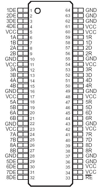
Pinout

  Connection Diagram


Specifications

  SN65MLVD080, 082
Supply voltage range(2), VCC −0.5 V to 4 V
Input voltage range D, DE, RE −0.5 V to 4 V
A, B −1.8 V to 4 V
Output voltage range R −0.3 V to 4 V
A, or B −1.8 V to 4 V
Storage temperature range Human Body Model(3) A, B ±8 kV
All pins ±2 kV
Charged-Device Model(4) All pins ±1500 V
Continuous power dissipation See Dissipation Rating Table
Storage temperature range −65°C to 150°C


Description

The SN65MLVD080 and SN65MLVD082 provide eight half-duplex transceivers for transmitting and receiving Multipoint-Low-Voltage Differential Signals in full compliance with the TIA/EIA-899 (M-LVDS) standard, which are optimized to operate at signaling rates up to 250Mbps. The driver outputs of SN65MLVD080 and SN65MLVD082 have been designed to support multipoint buses presenting loads as low as 30-Ω and incorporates controlled transition times to allow for stubs off of the backbone transmission line.

The M-LVDS standard defines two types of receivers, designated as Type-1 and Type-2. Type-1 receivers (SN65MLVD080) have thresholds of SN65MLVD080 and SN65MLVD082 centered about zero with 25 mV of hysteresis to prevent output oscillations with loss of input; Type-2 receivers (SN65MLVD082) implement a failsafe by using an offset threshold. In addition, the driver rise and fall times are between 1 and 2.0 ns, complying with the M-LVDS standard to provide operation at 250 Mbps while also accommodating stubs on the bus. Receiver outputs are slew rate controlled to reduce EMI and crosstalk effects associated with large current surges. The M-LVDS standard SN65MLVD080 and SN65MLVD082 allows for 32 nodes on the bus providing a high-speed replacement for RS-485 where lower common-mode can be tolerated or when higher signaling rates are needed.

The driver logic inputs and the receiver logic outputs of SN65MLVD080 and SN65MLVD082 are on separate pins rather than tied together as in some transceiver designs. The drivers have separate enables (DE) and the receivers are enabled globally through (RE). This arrangement of separate logic inputs, logic outputs, and enable pins allows for a listen-while-talking operation. The SN65MLVD080 and SN65MLVD082 are characterized for operation from −40°C to 85°C.


Customers Who Bought This Item Also Bought

Margin,quality,low-cost products with low minimum orders. Secure your online payments with SeekIC Buyer Protection.
Motors, Solenoids, Driver Boards/Modules
Crystals and Oscillators
Semiconductor Modules
Optical Inspection Equipment
View more