Features: ` Low-Voltage Differential 30 to 55 Line(1) Drivers and Receivers for Signaling Rates Up to 100 Mbps, Clock Frequencies up to 50 MHz
` Type-1 Receivers Incorporate 25 mV of Hysteresis (200A, 202A)
` Type-2 Receivers Provide an Offset(100 mV) Threshold to Detect Open-Circuit and Idle-Bus Conditions (204A, 205A)
`Meets or Exceeds the M-LVDS Standard TIA/EIA-899 for Multipoint Data Interchange
` Power Up/Down Glitch Free
` Controlled Driver Output Voltage Transition Times for Improved Signal Quality
` -1 V to 3.4 V Common-Mode Voltage Range Allows Data Transfer With 2 V of Ground Noise
` Bus Pins High Impedance When Disabled or VCC 1.5 V 200-Mbps Devices Available (SN65MLVD201, 203, 206, 207)
` Bus Pin ESD Protection Exceeds 8 kV
`Package in 8-Pin SOIC (200A, 204A) and 14-Pin SOIC (202A, 205A)
` Improved Alternatives to the SN65MLVD200, 202, 204, and 205Application· Low-Power High-Speed Short-Reach Alternative to TIA/EIA-485
· Backplane or Cabled Multipoint Data and Clock Transmission
· Cellular Base Stations
· Central-Office Switches
· Network Switches and Routers
(1) The signaling rate of a line, is the number of voltage transitions that are made per second expressed in the nits bps (bits per second).
Pinout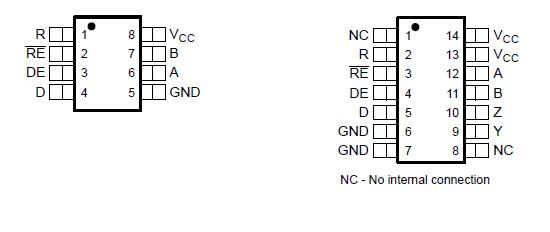 Specifications
| |
SN65MLVD200A,
202A, 204A, and 205A |
| Supply voltage range(2), VCC |
0.5 V to 4 V |
| Input voltage range |
D, DE, RE |
0.5 V to 4 V |
| A, B (200A, 204A) |
1.8 V to 4 V |
| A, B (202A, 205A) |
4 V to 6 V |
| Output voltage range |
R |
0.3 V to 4 V |
| Y, Z, A, or B |
1.8 V to 4 V |
| Electrostatic discharge |
Human Body Model(3) |
A, B, Y, and Z |
±8 kV |
| All pins |
±4 kV |
| Charged-Device Model(4) |
All pins |
±1500 V |
| Continuous power dissipation |
See Dissipation Rating Table |
| Storage temperature range |
65°C to 150°C |
(1) Stresses beyond those listed under absolute maximum ratings may cause permanent damage to the device. These are stress ratings only, and functional operation of the device at these or any other conditions beyond those indicated under recommended operating conditions is not implied. Exposure to absolute-maximum-rated conditions for extended periods may affect device reliability.
(2) All voltage values, except differential I/O bus voltages, are with respect to network ground terminal.
(3) Tested in accordance with JEDEC Standard 22, Test Method A114-A.
(4) Tested in accordance with JEDEC Standard 22, Test Method C101.
DescriptionThe SN65MLVD200A, 202A, 204A, and 205A are multipoint-low-voltage differential (M-LVDS) line drivers and receivers, which are optimized to operate at signaling rates up to 100 Mbps. All parts comply with the multipoint low-voltage differential signaling (M-LVDS) standard TIA/EIA-899. SN65MLVD200A, 202A, 204A, and 205A are similar to their TIA/EIA-644 standard compliant LVDS counterparts, with added features to address multipoint applications. The driver output has been designed to support multipoint buses presenting loads as low as 30 , and incorporates controlled transition times to allow for stubs off of the backbone transmission line.
SN65MLVD200A, 202A, 204A, and 205A have Type-1 and Type-2 receivers that detect the bus state with as little as 50 mV of differential input voltage over a common-mode voltage range of - 1 V to 3.4 V. The Type-1 receivers exhibit 25 mV of differential input voltage hysteresis to prevent output oscillations with slowly changing signals or loss of input. Type-2 receivers include an offset threshold of SN65MLVD200A, 202A, 204A, and 205A to provide a known output state under open-circuit, idle-bus, and other fault conditions.
The SN65MLVD200A, 202A, 204A, and 205A have enhancements over their predecessors. Improved features include better controlled slew rate on the driver output to help minimize reflections while improving overall signal integrity (SI) resulting in better jitter performance. Additionally, 8-kV ESD protection on the bus pins for more robustness. The same footprint definition was maintained making for an easy drop-in replacement for a system performance upgrade.
The SN65MLVD200A, 202A, 204A, and 205A are characterized for operation from -40 to 85.

 SN65MLVD200A Data Sheet


