Features: • Members of the Texas Instruments SCOPETM Family of Testability Products
• Members of the Texas Instruments WidebusTM Family
• Compatible With the IEEE Standard 1149.1-1990 (JTAG) Test Access Port and Boundary-Scan Architecture
• Include D-Type Flip-Flops and Control Circuitry to Provide Multiplexed
• Two Boundary-Scan Cells per I/O for Greater Flexibility
• State-of-the-Art EPIC-II BTM BiCMOS Design Significantly Reduces Power Dissipation
• SCOPETM Instruction Set
IEEE Standard 1149.1-1990 Required Instructions, Optional INTEST, and P1149.1A CLAMP and HIGHZ
Parallel Signature Analysis at Inputs With Masking Option
Pseudo-Random Pattern Generation From Outputs
Sample Inputs/Toggle Outputs
Binary Count From Outputs
Device Identification
Even-Parity Opcodes
• Packaged in 64-Pin Plastic Shrink Quad Flat Pack (PM) and 68-Pin Ceramic Quad Flat Pack (HV)
Pinout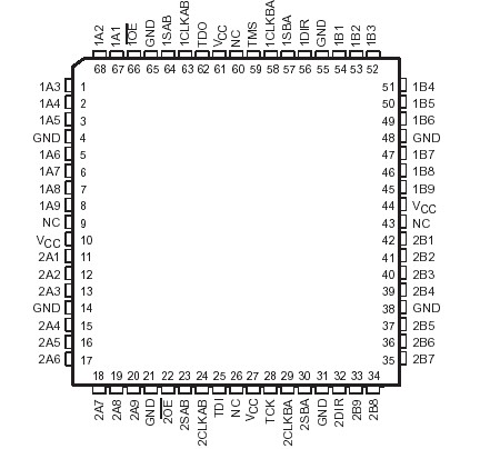 SpecificationsSupply voltage range, VCC . . . . . . . . . . . . . . . . . . . . . . . . . . . . . . . . . . . . . . . . . . . . . . . . . .0.5 V to 7 V
Input voltage range, VI (except I/O ports) (see Note 1) . . . . . . . . . . . . . . . . . . . .. . . . . . . . .0.5 V to 7 V
Input voltage range, VI (I/O ports) (see Note 1) . . . . . . . . . . . . . . . . . . . . . . . . . . . . . . . . .0.5 V to 5.5 V
Voltage range applied to any output in the high state or power-off state, VO . . . . . . . . . .0.5 V to 5.5 V
Current into any output in the low state, IO: SN54ABT18646 . . . . . . . . . . . . . . .. . . . . . . . . . . . . . .96 mA
SN74ABT18646 . . . . . . . . . . . . . . . . . . . . . . . . . . . . .128 mA
Input clamp current, IIK (VI < 0) . . . . . . . . . . . . . . . . . . . . . . . . . . . . . . . . . . . . . . . . . . . . . . . . . . . 18 mA
Output clamp current, IOK (VO < 0) . . . . . . . . . . . . . . . . . . . . . . . . . . . . . . . . .. . . . . . . . . . . . . . . . .50 mA
Maximum power dissipation at TA = 55°C (in still air) (see Note 2) . . . . . . . . . . . . . . . . . . . . . . . . .885 mW
Storage temperature range . . . . . . . . . . . . . . . . . . . . . . . . . . . . . . . . . . . . . . . . . . . . . . . .65°C to 150°C DescriptionThe SN54ABT18646 and SN74ABT18646 scan test devices with 18-bit bus transceivers and registers are members of the Texas Instruments SCOPETM testability IC family. This SN54ABT18646 and SN74ABT18646 supports IEEE Standard 1149.1-1990 boundary scan to facilitate testing of complex circuit board assemblies. Scan access to the test circuitry is accomplished via the 4-wire test access port (TAP) interface.
In the normal mode, theseSN54ABT18646 and SN74ABT18646 devices are 18-bit bus transceivers and registers that allow for multiplexed transmission of data directly from the input bus or from the internal registers. They can be used either as two 9-bit transceivers or one 18-bit transceiver. The test circuitry can be activated by the TAP to take snapshot samples of the data appearing at the device pins or to perform a self test on the boundary test cells. Activating the TAP in the normal mode does not affect the functional operation of the SCOPEE bus transceivers and registers.
Transceiver function of SN54ABT18646 and SN74ABT18646 is controlled by output-enable (OE) and direction (DIR) inputs. When OE is low, the transceiver is active and operates in the A-to-B direction when DIR is high or in the B-to-A direction when DIR is low. When OE is high, both the A and B outputs are in the high-impedance state, effectively isolating both buses.
Data flow of SN54ABT18646 and SN74ABT18646 is controlled by clock (CLKAB and CLKBA) and select (SAB and SBA) inputs. Data on the A bus is clocked into the associated registers on the low-to-high transition of CLKAB. When SAB is low, real-time A data is selected for presentation to the B bus (transparent mode). When SAB is high, stored A data is selected for presentation to the B bus (registered mode). The function of the CLKBA and SBA inputs mirrors that of CLKAB and SAB, respectively. Figure 1 illustrates the four fundamental bus-management functions that can be performed with the 4ABT18646.
In the test mode, the normal operation of the SN54ABT18646 and SN74ABT18646 SCOPETM bus transceivers and registers is inhibited, and the test circuitry is enabled to observe and control the I/O boundary of the device. When enabled, the test circuitry can perform boundary scan test operations according to the protocol described in IEEE Standard 1149.1-1990.
Four dedicated test pins are used to observe and control the operation of the test circuitry: test data input (TDI), test data output (TDO), test mode select (TMS), and test clock (TCK). Additionally, the test circuitry can perform other testing functions such as parallel signature analysis on data inputs and pseudo-random pattern generation from data outputs. All testing and scan operations are synchronized to the TAP interface.Additional flexibility is provided in the test mode through the use of two boundary scan cells (BSCs) for each I/O pin. SN54ABT18646 and SN74ABT18646 allows independent test data to be captured and forced at either bus (A or B). A PSA/COUNT instruction is also included to ease the testing of memories and other circuits where a binary count addressing scheme is useful.The SN54ABT18646 is characterized over the full military temperature range of 55°C to 125°C. The SN74ABT18646 is characterized for operation from 40°C to 85°C.

 SN74ABT18646 Data Sheet


