Features: • State-of-the-Art EPIC-II BTM BiCMOS Design Significantly Reduces Power Dissipation
• Latch-Up Performance Exceeds 500 mA Per JEDEC Standard JESD-17
• Typical VOLP (Output Ground Bounce) < 1 V at VCC = 5 V, TA = 25°C
• High-Drive Outputs (32-mA IOH, 64-mA IOL)
• Package Options Include Plastic Small-Outline (DW), Shrink Small-Outline (DB), and Thin Shrink Small-Outline (PW) Packages, Ceramic Chip Carriers (FK), and Plastic (N) and Ceramic (J) DIPs
Pinout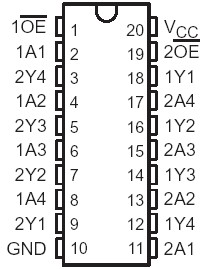 SpecificationsSupply voltage range, VCC . . . . . . . . . . . . . . . . . . . . . . . . . . . . . . . . . . . . . . . . . . . . . . 0.5 V to 7 V
Input voltage range, VI (except I/O ports) (see Note 1) . . . . . . . . . . . . . . . . . . . . . . . . .0.5 V to 7 V
Voltage applied to any output in the high state or power-off state, VO . . . . . . . . . .0.5 V to 5.5 V
Current into any output in the low state, IO: SN54ABT244 . . . . . . . . . . . . .. . . . . . . . . . . . .. . .96 mA
SN74ABT244 . . . . . . . . . . . . . . . . . . . . . . . .. .128 mA
Input clamp current, IIK (VI < 0) . . . . . . . . . . . . . . . . . . . . . . . . . . . . . . . .. . . . . . . . . . . . . . .. .18 mA
Output clamp current, IOK (VO < 0) . . . . . . . . . . . . . . . . . . . . . . . . . . . . . . . . . . . . . . . . . . . . .50 mA
Maximum power dissipation at TA = 55°C (in still air) (see Note 2): DB package . . . . . . . . . . .0.6 W
DW package . . . .. . . . . .. .1.6 W
N package . . . .. . . . . . . . . .1.3 W
PW package . . . . . . . . . . . .0.7 W
Storage temperature range . . . . . . . . . . . . . . . . . . . . . . . . . . . . . . . . . . . . . . . . .. . . .65°C to 150°C DescriptionThese SN74ABT244 octal buffers and line drivers are designed specifically to improve both the performance and density of 3-state memory address drivers, clock drivers, and bus-oriented receivers and transmitters. Taken together with the 4ABT240 and 4ABT241, these devices provide the choice of selected combinations of inverting and noninverting outputs, symmetrical active-low output-enable (OE) inputs, and complementary OE and OE inputs.
The SN74ABT244 is organized as two 4-bit buffers/line drivers with separate OE inputs. When OE is low, the device passes data from the A inputs to the Y outputs. When OE is high, the outputs are in the high-impedance state.
To ensure the high-impedance state of SN74ABT244 during power up or power down, OE should be tied to VCC through a pullup resistor; the minimum value of the resistor is determined by the current-sinking capability of the driver.
The SN74ABT244 is available in TI's shrink small-outline package (DB), which provides the same I/O pin count and functionality of standard small-outline packages in less than half the printed-circuit-board area.
The SN54ABT244 is characterized for operation over the full military temperature range of 55°C to 125°C. The SN74ABT244 is characterized for operation from 40°C to 85°C.

 SN74ABT244 Data Sheet


