Features: · Low-Power Advanced BiCMOS Technology
· Free-Running CLKA and CLKB Can Be Asynchronous or Coincident
· 64 × 36 FIFO Buffering Data From Port A to Port B
· Mailbox-Bypass Registers in Each Direction
· Dynamic Port-B Bus Sizing of 36 Bits (Long Word), 18 Bits (Word), and 9 Bits (Byte)
·Selection of Big- or Little-Endian Format for Word and Byte Bus Sizes
· Three Modes of Byte-Order Swapping on Port B
· Programmable Almost-Full and Almost-Empty Flags
· Microprocessor Interface Control Logic
· FF and AF Flags Synchronized by CLKA
· EF and AE Flags Synchronized by CLKB
· Passive Parity Checking on Each Port
· Parity Generation Can Be Selected for Each Port
· Supports Clock Frequencies up to 67 MHz
· Fast Access Times of 10 ns
· Package Options Include 120-Pin Thin Quad Flat (PCB) and 132-Pin Quad Flat (PQ) PackagesPinout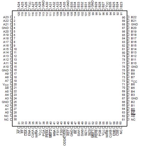 Specifications
Supply voltage range, VCC . . . . . . . . . . . . . . . . . . . . . . . . . . . . . . . . . . . . . . . . . . 0.5 V to 7 V
Input voltage range, VI (see Note 1) . . . . . . . . . . . . . . . . . . . . . . . . . . . 0.5 V to VCC + 0.5 V
Output voltage range, VO (see Note 1) . . . . . . . . . . . . . . . . . . . . . . . .. . 0.5 V to VCC + 0.5 V
Input clamp current, IIK (VI < 0 or VI > VCC) . . . . . . . . . . . . . . . . . . . . . . . . . . . .. . . . . ±20 mA
Output clamp current, IOK (VO < 0 or VO > VCC) . . . . . . . . . . . . . . . . . . . . . . . . . .. . . . ±50 mA
Continuous output current, IO (VO = 0 to VCC) . . . . . . . . . . . . . . . . . . . . . . . . . . . . . . ±50 mA
Continuous current through VCC or GND . . . . . . . . . . . . . . . . . . . . . . . . . . . . . . . . . .. ±500 mA
Package thermal impedance, JA (see Note 2): PCB package . . . . . . . . . . . . . . . . . . . 28°C/W
PQ package . . . . . . . . .. . . . . . . . . . . . 46°C/W
Storage temperature range, Tstg . . . . . . . . . . . . . . . . . . . . . . . . . . . . . . . . . 65°C to 150°C
† Stresses beyond those listed under "absolute maximum ratings" may cause permanent damage to the device. These are stress ratings only, and functional operation of the device at these or any other conditions beyond those indicated under "recommended operating conditions" is not implied. Exposure to absolute-maximum-rated conditions for extended periods may affect device reliability.
NOTES: 1. The input and output voltage ratings may be exceeded provided the input and output current ratings are observed.
2. The package thermal impedance is calculated in accordance with JESD 51.
DescriptionThe SN74ABT3613 is a high-speed, low-power BiCMOS clocked FIFO memory. It supports clock frequencies up to 67 MHz and has read-access times as fast as 10 ns. A 64 × 36 dual-port SRAM FIFO in this device buffers data from port A to port B. The FIFO has flags to indicate empty and full conditions and two programmable flags (almost full and almost empty) to indicate when a selected number of words is stored in memory. FIFO data on port B can be output in 36-bit, 18-bit, and 9-bit formats, with a choice of big- or little-endian configurations. Three modes of byte-order swapping are possible with any bus-size selection. Communication between each port can bypass the FIFO via two 36-bit mailbox registers. Each mailbox register has a flag to signal when new mail has been stored. Parity is checked passively on each port and can be ignored if not desired. Parity generation can be selected for data read from each port.
The SN74ABT3613 is a clocked FIFO, which means each port employs a synchronous interface. All data transfers through a port are gated to the low-to-high transition of a continuous (free-running) port clock by enable signals. The continuous clocks for each port are independent of one another and can be asynchronous or coincident. The enables for each port are arranged to provide a simple interface between microprocessors and/or buses controlled by a synchronous interface.
The full flag (FF) and almost-full (AF) flag of a FIFO are two-stage synchronized to the port clock that writes data to its array. The empty flag (EF) and almost-empty (AE) flag of a FIFO are two-stage synchronized to the port clock that reads data from its array.The SN74ABT3613 is characterized for operation from 0°C to 70°C.
For more information on SN74ABT3613, see the following application reports:
· FIFO Mailbox-Bypass Registers: Using Bypass Registers to Initialize DMA Control (literature number SCAA007)
· Advanced Bus-Matching/Byte-Swapping Features for Internetworking FIFO Applications (literature number SCAA014)
· Parity-Generate and Parity-Check Features for High-Bandwidth-Computing FIFO Applications (literature number SCAA015)
· Internetworking the SN74ABT3614 (literature number SCAA018)
· Metastability Performance of Clocked FIFOs (literature number SCZA004)

 SN74ABT3613 Data Sheet


