Features: State-of-the-Art EPIC-II BTM BiCMOS Design Significantly Reduces Power Dissipation
ESD Protection Exceeds 2000 V Per MIL-STD-883, Method 3015; Exceeds 200 V Using Machine Model (C = 200 pF, R = 0)
Latch-Up Performance Exceeds 500 mA Per JEDEC Standard JESD-17
Typical VOLP (Output Ground Bounce) < 1 V at VCC = 5 V, TA = 25°C
High-Drive Outputs (32-mA IOH, 64-mA IOL)
Package Options Include Plastic Small-Outline (DW), Shrink Small-Outline (DB), and Thin Shrink Small-Outline (PW) Packages, Ceramic Chip Carriers (FK), Plastic (N) and Ceramic (J) DIPs, and Ceramic Flat (W) Packages
Application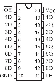 SpecificationsSupply voltage range, VCC . . . . . . . . . . . . . . . . . . . . . . . . . . . . . . . . . . . . . . . . . . . . . . 0.5 V to 7 V
Input voltage range, VI(see Note 1) . . . . . . . . . . . . . . . . . . . . . . . . .. . .. . . . . . . . . . .0.5 V to 7 V
Voltage applied to any output in the high state or power-off state, VO . . . . . . . . . .0.5 V to 5.5 V
Current into any output in the low state, IO: SN54ABT573 . . . . . . . . . . . . .. . . . . . . . . . . . .. . .96 mA
SN74ABT573A . . . . . . . . . . . . . . . .. . . . . . . .. .128 mA
Input clamp current, IIK (VI < 0) . . . . . . . . . . . . . . . . . . . . . . . . . . . . . . . .. . . . . . . . . . . . . . .. .18 mA
Output clamp current, IOK (VO < 0) . . . . . . . . . . . . . . . . . . . . . . . . . . . . . . . . . . . . . . . . . . . . .50 mA
Package thermal impedance, JA (see Note 2): DB package . . . . . . . . . . . . . . . . . . . . . . .115°C/W
DW package . . . .. . . . . . . . . . . . . . . . . . . .. .97°C/W
N package . . . .. . . . . . . . . . . . . . . . . . . . . . . 67°C/W
PW package . . . . . . . . . . . . . . . . . . . . . . .. .128°C/W
Storage temperature range, Tstg . . . . . . . . . . . . . . . . . . . . . . . . . . . . . . . . . . . .. . . .65°C to 150°C DescriptionThese SN54ABT573 and SN74ABT573A 8-bit latches feature 3-state outputs designed specifically for driving highly capacitive or relatively low-impedance loads. They are particularly suitable for implementing buffer registers, I/O ports, bidirectional bus drivers, and working registers.
The eight latches of the SN54ABT573 and SN74ABT573A are transparent D-type latches. While the latch-enable (LE) input is high, the Q outputs follow the data (D) inputs. When LE is taken low, the Q outputs are latched at the logic levels set up at the D inputs.
A buffered output-enable (OE) input of SN54ABT573 and SN74ABT573A can be used to place the eight outputs in either a normal logic state (high or low logic levels) or a high-impedance state. In the high-impedance state, the outputs neither load nor drive the bus lines significantly. The high-impedance state and increased drive provide the capability to drive bus lines without need for interface or pullup components.
OE does not affect the internal operations of the latches. Old data can be retained or new data can be entered while the outputs are in the high-impedance state. To ensure the high-impedance state of SN54ABT573 and SN74ABT573A during power up or power down, OE should be tied to VCC through a pullup resistor; the minimum value of the resistor is determined by the current-sinking capability of the driver.The SN54ABT573 is characterized for operation over the full military temperature range of 55°C to 125°C. The SN74ABT573A is characterized for operation from 40°C to 85°C.

 SN74ABT573A Data Sheet


