Features: · Member of the Texas Instruments WidebusE Family
· Free-Running CLKA and CLKB Can Be Asynchronous or Coincident
· Read and Write Operations Synchronized to Independent System Clocks
· Two Separate 512 × 18 Clocked FIFOs Buffering Data in Opposite Directions
· IRA and ORA Synchronized to CLKA
· IRB and ORB Synchronized to CLKB
· Microprocessor Interface Control Logic
· Programmable Almost-Full/Almost-Empty Flag
· Fast Access Times of 9 ns With a 50-pF Load and Simultaneous Switching Data Outputs
· Data Rates up to 100 MHz
· Advanced BiCMOS Technology
· Package Options Include 80-Pin Quad Flat (PH) and 80-Pin Thin Quad Flat (PN) PackagesPinout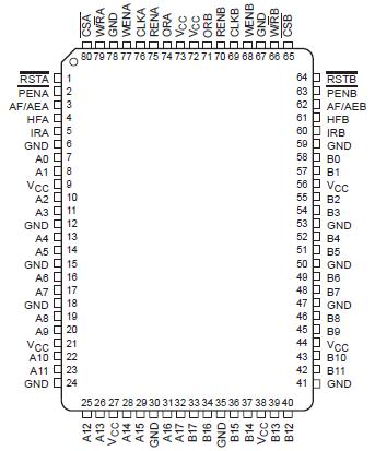 Specifications
Supply voltage range, VCC . . . . . . . . . . . . . . . . . . . . . . . . . . . . . . . . . . . . . . . . . . . . . . . . . . . . . . . . . . 0.5 V to 7 V
Input voltage range, VI (see Note 1) . . . . . . . . . . . . . . . . . . . . . . . . . . . . . . . . . . . . . . . . . . . 0.5 V to VCC + 0.5 V
Voltage range applied to any output in the high state or power-off state, VO . . . . . . . . . . . . . . 0.5 V to 5.5 V
Current into any output in the low state, IO . . . . . . . . . . . . . . . . . . . . . . . . . . . . . . . . . . . . . . . . . . . . . . . . . . 48 mA
Input clamp current, IIK (VI < 0) . . . . . . . . . . . . . . . . . . . . . . . . . . . . . . . . . . . . . . . . . . . . . . . . . . . . . . . . . . . 18 mA
Output clamp current, IOK (VO < 0) . . . . . . . . . . . . . . . . . . . . . . . . . . . . . . . . . . . . . . . . . . . . . . . . . . . . . . . . 50 mA
Package thermal impedance, qJA (see Note 2): PH package . . . . . . . . . . . . . . . . . . . . . . . . . . . . . . . . . . 76°C/W
PN package . . . . . . . . . . . . . . . . . . . . . . . . . . . . . . . . . . 62°C/W
Storage temperature range, Tstg . . . . . . . . . . . . . . . . . . . . . . . . . . . . . . . . . . . . . . . . . . . . . . . . . . . 65°C to 150°C
† Stresses beyond those listed under "absolute maximum ratings" may cause permanent damage to the device. These are stress ratings only, and functional operation of the device at these or any other conditions beyond those indicated under "recommended operating conditions" is not implied. Exposure to absolute-maximum-rated conditions for extended periods may affect device reliability.
NOTES:
1. The input and output negative-voltage ratings may be exceeded if the input and output clamp-current ratings are observed.
2. The package thermal impedance is calculated in accordance with JESD 51.
DescriptionA FIFO memory is a storage device that allows data to be written into and read from its array at independent
data rates. The SN74ABT7819 is a high-speed, low-power BiCMOS bidirectional clocked FIFO memory. Two
independent 512 * 18 dual-port SRAM FIFOs on the chip buffer data in opposite directions. Each FIFO has flags
to indicate empty and full conditions, a half-full flag, and a programmable almost-full/almost-empty flag.
The SN74ABT7819 is a clocked FIFO, which means each port employs a synchronous interface. All data
transfers through a port are gated to the low-to-high transition of a continuous (free-running) port clock by enable signals. The continuous clocks for each port are independent of one another and can be asynchronous or coincident. The enables for each port are arranged to provide a simple bidirectional interface between microprocessors and/or buses with synchronous control.
The state of the SN74ABT7819 outputs is controlled by CSA and W/RA. When both CSA and W/RA are low, the outputs are active. The A0A17 outputs are in the high-impedance state when either CSA or W/RA is high. Data is written to IFOAB from port A on the low-to-high transition of CLKA when CSA is low, W/RA is high, WENA is high, and the IRA flag is high. Data is read from FIFOBA to the A0A17 outputs on the low-to-high transition of CLKA when CSA is low, W/RA is low, RENA is high, and the ORA flag is high.

 SN74ABT7819 Data Sheet


