Features: ` State-of-the-Art EPIC-IIBTM BiCMOS Design Significantly Reduces Power Dissipation
` ESD Protection Exceeds 2000 V Per MIL-STD-883, Method 3015; Exceeds 200 V Using Machine Model (C = 200 pF, R = 0)
` Latch-Up Performance Exceeds 500 mA Per JEDEC Standard JESD-17
` Typical VOLP (Output Ground Bounce) < 1 V at VCC = 5 V, TA = 25°C
` High-Impedance State During Power Up and Power Down
` High-Drive Outputs (32-mA IOH, 64-mA IOL)
` Buffered Control Inputs to Reduce dc Loading Effects
` Package Options Include Plastic Small-Outline (DW) and Shrink Small-Outline (DB) Packages, Ceramic Chip Carriers (FK) and Flatpacks (W), and Standard Plastic (NT) and Ceramic (JT) DIPs
Pinout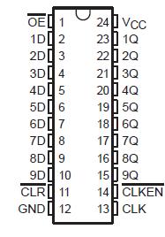
SpecificationsSupply voltage range, VCC . . . . . . . . . . . . . . . . . . . . . . . . . . . . . . . . . . . . . . . . . . . . 0.5 V to 7 V
Input voltage range, VI (see Note 1) . . . . . . . . . . . . . . . . . . . . . . . . . . . . . . . . . . . . 0.5 V to 7 V
Voltage range applied to any output in the high or power-off state, VO . . . . . . . . 0.5 V to 5.5 V
Current into any output in the low state, IO: SN54ABT823 . . . . . . . . . . . . . . . . . . . . . . . . . 96 mA
SN74ABT823 . . . . . . . . . . . . . . . . . . . . . . . . 128 mA
Input clamp current, IIK (VI < 0) . . . . . . . . . . . . . . . . . . . . . . . . . . . . . . . . . . . . . . . . . . . . 18 mA
Output clamp current, IOK (VO < 0) . . . . . . . . . . . . . . . . . . . . . . . . . . . . . . . . . . . . . . . . . . 50 mA
Package thermal impedance, JA (see Note 2): DB package . . . . . . . . . . . . . . . . . . . . . . 104°C/W
DW package . . . . . . . . . . . . . . . . . . . . . . . 81°C/W
NT package . . . . . . . . . . . . . . . . . . . . . . . . 67°C/W
Storage temperature range, Tstg . . . . . . . . . . . . . . . . . . . . . . . . . . . . . . . . . . . . 65°C to 150°C
† Stresses beyond those listed under "absolute maximum ratings" may cause permanent damage to the device. This is a stress rating only, and functional operation of the device at these or any other conditions beyond those indicated in the "recommended operating conditions" section of this specification is not implied. Exposure to absolute-maximum-rated conditions for extended periods may affect device reliability.
NOTES: 1. The input and output negative-voltage ratings may be exceeded if the input and output clamp-current ratings are observed.
2. The package thermal impedance is calculated in accordance with EIA/JEDEC Std JESD51, except for through-hole packages, which use a trace length of zero.
DescriptionThese SN74ABT823 9-bit flip-flops feature 3-state outputs designed specifically for driving highly capacitive or relatively low-impedance loads. They are particularly suitable for implementing wider buffer registers, I/O ports, bidirectional bus drivers with parity, and working registers.
With the clock-enable (CLKEN) input of SN74ABT823 low, the nine D-type edge-triggered flip-flops enter data on the low-to-high transitions of the clock. Taking CLKEN high disables the clock buffer, thus latching the outputs. Taking the clear (CLR) input low causes the nine Q outputs to go low, independently of the clock.
A buffered output-enable (OE) input of SN74ABT823can be used to place the nine outputs in either a normal logic state (high or low logic level) or a high-impedance state. In the high-impedance state, the outputs neither load nor drive the bus lines significantly. The high-impedance state and increased drive provide the capability to drive bus lines without need for interface or pullup components.
When VCC is between 0 and 2.1 V, the SN74ABT823 device is in the high-impedance state during power up or power down. However, to ensure the high impedance state above 2.1 V, OE should be tied to VCC through a pullup resistor; the minimum value of the resistor is determined by the current sinking capability of the driver.
The SN54ABT823 is characterized for operation over the full military temperature range of 55°C to 125°C. The SN74ABT823 is characterized for operation from 40°C to 85°C.

 SN74ABT823 Data Sheet


