Features: ` State-of-the-Art EPIC-IIBTM BiCMOS Design Significantly Reduces Power Dissipation
` ESD Protection Exceeds 2000 V Per MIL-STD-883, Method 3015; Exceeds 200 V Using Machine Model (C = 200 pF, R = 0)
` Latch-Up Performance Exceeds 500 mA Per JEDEC Standard JESD-17
` Typical VOLP (Output Ground Bounce) < 1 V at VCC = 5 V, TA = 25°C
` High-Drive Outputs (32-mA IOH, 64-mA IOL)
` Parity Error Flag With Parity Generator/Checker
` Register for Storage of the Parity Error Flag
` Package Options Include Plastic Small-Outline (DW) Packages, Ceramic Chip Carriers (FK), and Plastic (NT) and Ceramic (JT) DIPs
Pinout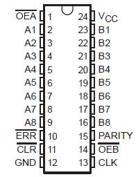
SpecificationsSupply voltage range, VCC . . . . . . . . . . . . . . . . . . . . . . . . . . . . . . . . . . .. . . . . . . . . . 0.5 V to 7 V
Input voltage range, VI (except I/O ports) (see Note 1) . . . . . . . . . . . . . . . . . . . . . . 0.5 V to 7 V
Voltage range applied to any output in the high or power-off state, VO . . . . . . . . .0.5 V to 5.5 V
Current into any output in the low state, IO: SN54ABT833 . . . . . . . . . . . . . . . . . . . . . . . . . . 96 mA
SN74ABT833 . . . . . . . . . . . . . . . . . . . . . . . . . 128 mA
Input clamp current, IIK (VI < 0) . . . . . . . . . . . . . . . . . . . . . . . . . . . . . . . . . . . . . . .. . . .. . . 18 mA
Output clamp current, IOK (VO < 0) . . . . . . . . . . . . . . . . . . . . . . . . . . . . . . .. . . . . . . . . . . . 50 mA
Package thermal impedance, JA (see Note 2): DW package . . . . . . . . . . . . . . . . . . . . . . . 81°C/W
NT package . . . . . . . . . . . . . . . . . . . . . . . . 67°C/W
Storage temperature range, Tstg . . . . . . . . . . . . . . . . . . . . . . . . . . . . . . . . . . . . . 65°C to 150°C
† Stresses beyond those listed under "absolute maximum ratings" may cause permanent damage to the device. These are stress ratings only, and
functional operation of the device at these or any other conditions beyond those indicated under "recommended operating conditions" is not implied. Exposure to absolute-maximum-rated conditions for extended periods may affect device reliability.
NOTES: 1. The input and output negative-voltage ratings may be exceeded if the input and output clamp-current ratings are observed.
2. The package thermal impedance is calculated in accordance with EIA/JEDEC Std JESD51, except for through-hole packages, which use a trace length of zero.
DescriptionThe 'ABT833 8-bit to 9-bit parity transceivers are designed for communication between data buses. When data is transmitted from the A bus to the
B bus, a parity bit is generated. When data is transmitted from the B bus to the A bus with its corresponding parity bit, the open-collector parity-error (ERR) output indicates whether or not an error in the B data has occurred. The output-enable (OEA and OEB) inputs can be used to disable the device so that the buses are effectively isolated. The 'ABT833 provide true data at their outputs.
A 9-bit parity generator/checker generates a parity-odd (PARITY) output and monitors the parity of the I/O ports with the ERR flag. ERR is clocked into the register on the rising edge of the clock (CLK) input. The 'ABT833 error flag register is cleared with a low pulse on the clear (CLR) input. When both OEA and OEB are low, data is transferred from the A bus to the B bus and inverted parity is generated. Inverted parity is a forced error condition that gives the designer more system diagnostic capability.

 SN74ABT833 Data Sheet


