SN74ABTE16246

Features: Members of the Texas Instruments WidebusTM FamilyState-of-the-Art EPIC-IIBTM BiCMOS Design Significantly Reduces Power DissipationSupport the VME64 ETL SpecificationReduced TTL-Compatible Input Threshold RangeHigh-Drive Outputs (IOH = 60 mA IOL = 90 mA) Support Equivalent 25- Incident-Wa...

product image

SN74ABTE16246 Picture
SeekIC No. : 004497849 Detail

SN74ABTE16246: Features: Members of the Texas Instruments WidebusTM FamilyState-of-the-Art EPIC-IIBTM BiCMOS Design Significantly Reduces Power DissipationSupport the VME64 ETL SpecificationReduced TTL-Compatible ...

floor Price/Ceiling Price

Part Number:
SN74ABTE16246
Supply Ability:
5000

Price Break

  • Qty
  • 1~5000
  • Unit Price
  • Negotiable
  • Processing time
  • 15 Days
Total Cost: $ 0.00

SeekIC Buyer Protection PLUS - newly updated for 2013!

  • Escrow Protection.
  • Guaranteed refunds.
  • Secure payments.
  • Learn more >>

Month Sales

268 Transactions

Rating

evaluate  (4.8 stars)

Upload time: 2025/12/24

Payment Methods

All payment methods are secure and covered by SeekIC Buyer Protection PLUS.

Notice: When you place an order, your payment is made to SeekIC and not to your seller. SeekIC only pays the seller after confirming you have received your order. We will also never share your payment details with your seller.
Product Details

Description


Features:

Members of the Texas Instruments WidebusTM Family
State-of-the-Art EPIC-IIBTM BiCMOS Design Significantly Reduces Power Dissipation
Support the VME64 ETL Specification
Reduced TTL-Compatible Input Threshold Range
High-Drive Outputs (IOH = 60 mA IOL = 90 mA) Support Equivalent 25- Incident-Wave Switching
VCCBIAS Pin Minimizes Signal Distortion During Live Insertion
Internal Pullup Resistor on OE Keeps Outputs in High-Impedance State During Power Up or Power Down
Distributed VCC and GND Pin Configuration Minimizes High-Speed Switching Noise
Equivalent 25- Series Damping Resistor on B Port
Bus Hold on Data Inputs Eliminates the Need for External Pullup/Pulldown Resistors
Package Options Include Plastic Shrink Small-Outline (DL) and Thin-Shrink Small-Outline (DGG) Packages and 380-mil Fine-Pitch Ceramic Flat (WD) Package Using 25-mil Center-to-Center Spacings


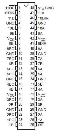
Pinout

  Connection Diagram


Specifications

Supply voltage range, VCC . . . . . . . . . . . . . . . . . . . . . . . . . . . . . . . .. . . . . . . . .  . . 0.5 V to 7 V
Input voltage range, VI (except I/O ports) (see Note 1) . . . . . . . . . . . . . . . .. . . . . 0.5 V to 7 V
Voltage range applied to any output in the high or power-off state, VO . . . . .  .  0.5 V to 5.5 V
Current into any output in the low state, IO . . . . . . . . . . . . . . . . . . . . . . . . . . ..   .. . .. . . 128 mA
Input clamp current, IIK (VI < 0) . . . . . . . . . . . . . . . . . . . . . . . . . . . . . . . . . . . . . . .. . . . . 18 mA
Output clamp current, IOK (VO < 0) . . . . . . . . . . . . . . . . . . . . . . . . . . . . . . . . . . .   . .. . . . 50 mA
Package thermal impedance, JA (see Note 2): DGG package . . . . . . . . . . . . . . . . .. . .. . 89°C/W
                                                                          DL package . . . . . . . . . . . . . . . . .  . . . . . 94°C/W
Storage temperature range, Tstg . . . . . . . . . . . . . . . . . . . . . . . . . .. . . . . . . . . . 65°C to 150°C
† Stresses beyond those listed under "absolute maximum ratings" may cause permanent damage to the device. These are stress ratings only, and functional operation of the device at these or any other conditions beyond those indicated under "recommended operating conditions" is not implied. Exposure to absolute-maximum-rated conditions for extended periods may affect device reliability.

NOTES: 1. The input and output negative-voltage ratings may be exceeded if the input and output clamp-current ratings are observed.

             2. The package thermal impedance is calculated in accordance with JESD 51.


Description

The 'ABTE16246 devices are 11-bit noninverting transceivers designed for asynchronous two-way communication between buses. These 'ABTE16246 devices have open-collector and 3-state outputs. They allow data transmission from the A bus to the B bus or from the B bus to the A bus, depending on the logic level at the direction-control (DIR) input. The output-enable (OE ) input can be used to disable the device so that the buses are effectively isolated. When OE is low, the device is active.

The B port of 'ABTE16246 has an equivalent 25- series output resistor to reduce ringing. Active bus-hold inputs on the B port hold unused or floating inputs at a valid logic level.The A port provides for the precharging of the outputs via VCCBIAS, which establishes a voltage between 1.3 V and 1.7 V when VCC is not connected.The SN54ABTE16246 is characterized for operation over the full military temperature range of 55°C to 125°C.The SN74ABTE16246 is characterized for operation from 40°C to 85°C.


Customers Who Bought This Item Also Bought

Margin,quality,low-cost products with low minimum orders. Secure your online payments with SeekIC Buyer Protection.
Motors, Solenoids, Driver Boards/Modules
Inductors, Coils, Chokes
Cables, Wires
Test Equipment
Static Control, ESD, Clean Room Products
Audio Products
View more