Features: ` Members of the Texas Instruments Widebus+™ Family
` State-of-the-Art EPIC-IIB™ BiCMOS Design Significantly Reduces Power Dissipation
` Latch-Up Performance Exceeds 500 mA Per JEDEC Standard JESD-17
` Typical VOLP (Output Ground Bounce) < 0.8 V at VCC = 5 V, TA = 25°C
` High-Impedance State During Power Up and Power Down
` Released as DSCC SMD 5962-9557701NXD
` PZ Package Qualified for Military Per MIL-PRF-38535 (QML)
` Distributed VCC and GND Pin Configuration Minimizes High-Speed Switching Noise
` High-Drive Outputs (32-mA IOH, 64-mA IOL)
` Bus Hold on Data Inputs Eliminates the Need for External Pullup/Pulldown Resistors
` Package Options Include 100-Pin Plastic Thin Quad Flat (PZ) Package With 14 * 14-mm Body Using 0.5-mm Lead Pitch and Space-Saving 100-Pin Ceramic Quad Flat (HS) Package†
Pinout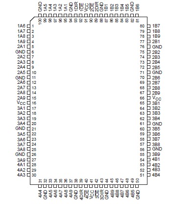
SpecificationsInput voltage range, VI (except I/O ports) (see Note 1) . . . . . . . . . . . . . . . . . . . . . . . 0.5 V to 7 V
Voltage range applied to any output in the high or power-off state, VO . . . . .. . . . . 0.5 V to 5.5 V
Current into any output in the low state, IO: SN54ABTH32245 . . . . . . . . . . . . . . . . . . . . . . . 96 mA
SN74ABTH32245 . . . . . . . . . . . . . . . .. . . . . . . 128 mA
Input clamp current, IIK (VI < 0) . . . . . . . . . . . . . . . . . . . . . . . . . . . . . . . . . . . . . .. . . . . . . . 18 mA
Output clamp current, IOK (VO < 0) . . . . . . . . . . . . . . . . . . . . . . . . . . . . . . . . . . . . . . . . . . . 50 mA
Package thermal impedance, JA (see Note 2): PZ package . . . . . . . . . . . . . . . . . . . . . . . . 50°C/W
Storage temperature range, Tstg . . . . . . . . . . . . . . . . . . . . . . . . . . . . . . . . . . . . . 65°C to 150°C
† Stresses beyond those listed under "absolute maximum ratings" may cause permanent damage to the device. These are stress ratings only, and functional operation of the device at these or any other conditions beyond those indicated under "recommended operating conditions" is not implied. Exposure to absolute-maximum-rated conditions for extended periods may affect device reliability. NOTES: 1. The input and output negative-voltage ratings may be exceeded if the input and output clamp-current ratings are observed. 2. The package thermal impedance is calculated in accordance with EIA/JEDEC Std JESD51.
DescriptionThe 'ABTH32245 are 36-bit (quad 9-bit) noninverting 3-state transceivers designed for synchronous two-way communication between data buses. The control-function implementation minimizes external timing requirements.
These 'ABTH32245 devices can be used as four 9-bit transceivers, two18-bit transceivers, or one 36-bit transceiver. They allow data transmission from the A bus to the B bus or from the B bus to the A bus, depending on the logic level at the direction-control (DIR) inputs. The output-enable (OE) inputs can be used to disable the device so that the buses are effectively isolated.
When VCC of 'ABTH32245 is between 0 and 2.1 V, the device is in the high-impedance state during power up or power down. However, to ensure the high-impedance state above 2.1 V,OE should be tied to VCC through a pullup resistor; the minimum value of the resistor is determined by the current-sinking capability of the driver.
Active bus-hold circuitry of 'ABTH32245 holds unused or floating data inputs at a valid logic level.

 SN74ABTH32245 Data Sheet


