Output Type
: 3-State
Supply Voltage - Max
: 5.5 V
Maximum Operating Temperature
: + 125 C
Packaging
: Reel
Logic Type
: Standard Transceiver
Supply Voltage - Min
: 4.5 V
Output Level
: CMOS
Input Level
: TTL
Number of Channels per Chip
: 16
Package / Case
: SSOP-48
High Level Output Current
: - 16 mA
Low Level Output Current
: 16 mA
Logic Family
: ACT
Propagation Delay Time
: 9.3 ns
Features: ` Controlled Baseline
One Assembly/Test Site, One Fabrication Site
` Extended Temperature Performance of
40°C to 125°C
` Enhanced Diminishing Manufacturing
Sources (DMS) Support
` Enhanced Product Change Notification
` Qualification Pedigree†
` Member of the Texas Instruments
Widebus Family
` Inputs Are TTL-Voltage Compatible
` 3-State Outputs Drive Bus Lines Directly
` Flow-Through Architecture Optimizes PCB Layout
` Distributed VCC and GND Pins Minimize
High-Speed Switching NoisePinout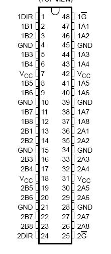 SpecificationsSupply voltage range, VCC . . . . . . . . . . . . . . . . . . . . . . . . . . . . . . . . . . . . . . . . . . . . . . . . . . . . . 0.5 V to 7 V
Input voltage range, VI (see Note 1) . . . . . . . . . . . . . . . . . . . . . . . . . . . . . . . . . . . . . . .0.5 V to VCC + 0.5 V
Output voltage range, VO (see Note 1) . . . . . . . . . . . . . . . . . . . . . . . . . . . . . . . . . . . . 0.5 V to VCC + 0.5 V
Input clamp current, IIK (VI < 0 or VI > VCC) . . . . . . . . . . . . . . . . . . . . . . . . . . . . . . . . . . . . . . . . . . . . ±20 mA
Output clamp current, IOK (VO < 0 or VO > VCC) . . . . . . . . . . . . . . . . . . . . . . . . . . . . . . . . . . . . . . . . . ±24 mA
Continuous output current, IO (VO = 0 to VCC) . . . . . . . . . . . . . . . . . . . . . . . . . . . . . . . . . . . . . . . . . . ±24 mA
Continuous current through VCC or GND . . . . . . . . . . . . . . . . . . . . . . . . . . . . . . . . . . . . . . . . . . . . . . ±260 mA
Maximum power dissipation at TA = 55°C (in still air) (see Note 2): DL package . . . . . . . . . . . . . . . . . . . 1.2 W
Storage temperature range, Tstg . . . . . . . . . . . . . . . . . . . . . . . . . . . . . . . . . . . . . . . . . . . . . . 65°C to 150°C
† Stresses beyond those listed under "absolute maximum ratings" may cause permanent damage to the device. These are stress ratings only, and
functional operation of the device at these or any other conditions beyond those indicated under "recommended operating conditions" is not
implied. Exposure to absolute-maximum-rated conditions for extended periods may affect device reliability.
NOTES: 1. The input and output voltage ratings may be exceeded if the input and output current ratings are observed.
2. The maximum package power dissipation is calculated using a junction temperature of 150°C and a board trace length of 750 mils.DescriptionThe SN74ACT16245Q-EP is a 16-bit bus transceiver organized as dual-octal noninverting3-state transceivers and designed for asynchronous two-way communication between data buses. The control-function implementation minimizes external timing requirements.
The SN74ACT16245Q-EP device allows data transmission from the A bus to the B bus or from the B bus to the A bus, depending on the logic level at the direction-control (DIR) input. The enable (G) input can be used to disable the devices so that the buses are effectively isolated.
Parameters: | Technical/Catalog Information | SN74ACT16245QDLREP |
| Vendor | Texas Instruments (VA) |
| Category | Integrated Circuits (ICs) |
| Logic Type | Transceiver, Non-Inverting |
| Package / Case | 48-SSOP |
| Packaging | Digi-Reel? |
| Mounting Type | Surface Mount |
| Number of Bits per Element | 8 |
| Number of Elements | 2 - Dual |
| Operating Temperature | -40°C ~ 125°C |
| Voltage - Supply | 4.5 V ~ 5.5 V |
| Current - Output High, Low | 16mA, 16mA |
| Drawing Number | 296; 4040048; DL; 28, 48, 56 |
| Lead Free Status | Contains Lead |
| RoHS Status | RoHS Non-Compliant |
| Other Names | SN74ACT16245QDLREP
SN74ACT16245QDLREP
296 18124 6 ND
296181246ND
296-18124-6
|

 SN74ACT16245QDLREP Data Sheet


