Pinout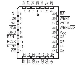 Specifications`Supply voltage range, VCC (see Note 1) . . . . . . . . . . . . . . . . . . . . . . . . . . . . . . . . . . . . . . . . . . . . . .0.5 V to 7 V
`Input voltage range, any input, VI (see Note 1) . . . . . . . . . . . . . . . . . . . . . . . . . . . . . . . . . . . . . . . . .0.5 V to 7 V
`Continuous output current, IO . . . . . . . . . . . . . . . . . . . . . . . . . . . . . . . . . . . . . . . . . . . . . . . . . . . . . . . . . .±50 mA
`Voltage applied to a disabled 3-state output . . . . . . . . . . . . . . . . . . . . . . . . . . . . . . . . . . . . . . . . . . . . . . . . . .5.5 V
`Operating free-air temperature range, TA . . . . . . . . . . . . . . . . . . . . . . . . . . . . . . . . . . . . . . . . . . . . . .0°C to 70°C
`Storage temperature range under bias . . . . . . . . . . . . . . . . . . . . . . . . . . . . . . . . . . . . . . . . . . . . .55°C to 125°C
`Storage temperature range . . . . . . . . . . . . . . . . . . . . . . . . . . . . . . . . . . . . . . . . . . . . . . . . . . . . .55°C to 125°CDescriptionThe SN74ACT72211L, SN74ACT72221L, SN74ACT72231L, and SN74ACT72241L are constructed with CMOS dual-port SRAM and are arranged as 512, 1024, 2048, and 4096 9-bit words, respectively. Internal write and read address counters provide data throughput on a first-in, first-out (FIFO) basis. Full and empty flags prevent memory overflow and underflow, and two programmable flags (almost full and almost empty) are provided.
The SN74ACT72211L, SN74ACT72221L, SN74ACT72231L, and SN74ACT72241L are synchronous FIFOs, which means the data input port and data output port each employ synchronous control. Write-enable (WEN1, WEN2/LD) signals allow the low-to-high transition of the write clock (WCLK)) to store data in memory, and read-enable (REN1, REN2) signals allow the low-to-high transition of the read clock( RCLK) to read data from memory. WCLK and RCLK are independent of one another and can operate asynchronously or be tied together
for single-clock operation.
The empty-flag (EF) output of SN74ACT72211L, SN74ACT72221L, SN74ACT72231L, and SN74ACT72241L is synchronized to RCLK and the full-flag (FF) output is synchronized to WCLK to indicate absolute boundary conditions. Write operations are prohibited when FF is low, and read operations are prohibited when EF is low. Two programmable flags, programmable almost empty (PAE) and programmable almost full (PAF), can both be programmed to indicate any measure of memory fill. After reset,PAE defaults
to empty+7 and PAF defaults to full7. Flag-offset programming control is similar to a memory write with the use of the load (WEN2/LD) signal.
These SN74ACT72211L, SN74ACT72221L, SN74ACT72231L, and SN74ACT72241L devices are suited for providing a data channel between two buses operating at asynchronous or synchronous rates. Applications include use as rate buffers for graphics systems and high-speed queues for communication systems. A 9-bit-wide data path is provided for the transmission of byte data plus a parity bit or packet-framing information.
The SN74ACT72211L, SN74ACT72221L, SN74ACT72231L, and SN74ACT72241L are characterized for operation from 0°C to 70°C.

 SN74ACT72241L Data Sheet


