Features: · Member of the Texas Instruments WidebusE Family
· Free-Running Read and Write Clocks Can Be Asynchronous or Coincident
· Read and Write Operations Synchronized to Independent System Clocks
· Input-Ready Flag Synchronized to Write Clock
· Output-Ready Flag Synchronized to Read Clock
· 512 Words by 18 Bits
· Low-Power Advanced CMOS Technology
· Half-Full Flag and Programmable Almost-Full/Almost-Empty Flag
· Bidirectional Configuration and Width Expansion Without Additional Logic
· Fast Access Times of 12 ns With a 50-pF Load and All Data Outputs Switching Simultaneously
· Data Rates up to 67 MHz
· Pin-to-Pin Compatible With SN74ACT7805 and SN74ACT7813
· Packaged in Shrink Small-Outline 300-mil Package Using 25-mil Center-to-Center SpacingPinout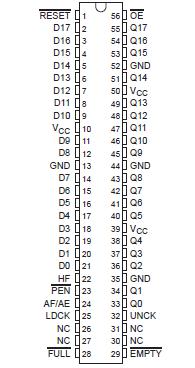 Specifications
Supply voltage range, VCC . . . . . . . . . . . . . . . . . . . . . . 0.5 V to 7 V
Input voltage range, VI . . . . . . . . . . . . . . . . . . . . . . . . . 0.5 V to 7 V
Voltage range applied to a disabled 3-state output . . 0.5 V to 5.5 V
Package thermal impedance, qJA (see Note 1) . . . . . . . . . . . .74°C/W
Storage temperature range, Tstg . . . . . . . . . . . . . . . 65°C to 150°C
DescriptionThe SN74ACT7803 is a 512-word × 18-bit FIFO suited for buffering asynchronous datapaths up to 67-MHz clock rates and 12-ns access times. Two devices can be configured for bidirectional data buffering without additional logic. Multiple distributed VCC and GND pins, along with Texas Instruments patented output edge control (OECE) circuit, dampen simultaneous switching noise.
The write clock (WRTCLK) and read clock (RDCLK) of SN74ACT7803 are free running and can be asynchronous or coincident. Data is written to memory on the rising edge of WRTCLK when WRTEN1 is high, WRTEN2 is low, and input ready (IR) is high. Data is read from memory on the rising edge of RDCLK when RDEN, OE1, and OE2 are low and output ready (OR) is high. The first word written to memory is clocked through to the output buffer, regardless of the RDEN, OE1, and OE2 levels. The OR flag indicates that valid data is present on the output buffer.
The SN74ACT7803 FIFO can be reset asynchronously to WRTCLK and RDCLK. RESET must be asserted while at least four WRTCLK and four RDCLK rising edges occur to clear the synchronizing registers. Resetting the FIFO initializes the IR, OR, and half-full (HF) flags low and the almost-full/almost-empty (AF/AE) flag high. The FIFO must be reset upon power up.
The SN74ACT7803 is characterized for operation from 0°C to 70°C.

 SN74ACT7803 Data Sheet


