SN74ACT8994

Features: · Member of the Texas Instruments SCOPE E Family of Testability Products· Compatible With the IEEE Standard 1149.1-1990 (JTAG) Test Access Port and Boundary-Scan Architecture· Contains a 1024-Word by 16-Bit Random-Access Memory (RAM) to Store the States of a Digital Bus· Test Operations ...

product image

SN74ACT8994 Picture
SeekIC No. : 004497950 Detail

SN74ACT8994: Features: · Member of the Texas Instruments SCOPE E Family of Testability Products· Compatible With the IEEE Standard 1149.1-1990 (JTAG) Test Access Port and Boundary-Scan Architecture· Contains a 1...

floor Price/Ceiling Price

Part Number:
SN74ACT8994
Supply Ability:
5000

Price Break

  • Qty
  • 1~5000
  • Unit Price
  • Negotiable
  • Processing time
  • 15 Days
Total Cost: $ 0.00

SeekIC Buyer Protection PLUS - newly updated for 2013!

  • Escrow Protection.
  • Guaranteed refunds.
  • Secure payments.
  • Learn more >>

Month Sales

268 Transactions

Rating

evaluate  (4.8 stars)

Upload time: 2025/12/24

Payment Methods

All payment methods are secure and covered by SeekIC Buyer Protection PLUS.

Notice: When you place an order, your payment is made to SeekIC and not to your seller. SeekIC only pays the seller after confirming you have received your order. We will also never share your payment details with your seller.
Product Details

Description


Features:

· Member of the Texas Instruments SCOPE E
  Family of Testability Products
· Compatible With the IEEE Standard
  1149.1-1990 (JTAG) Test Access Port and
  Boundary-Scan Architecture
· Contains a 1024-Word by 16-Bit
  Random-Access Memory (RAM) to Store
  the States of a Digital Bus
· Test Operations Are Synchronous to the
  Test Clock or System Clock(s)
· Contains Texas Instruments Event
  Qualification Module for Real-Time System Test
· Eight Protocols for On-Line Signal
  Monitoring and Test Operations
· Inputs Are TTL-Voltage Compatible
· Performs Parallel-Signature Analysis (PSA)
  of Data Inputs With User-Definable Feedback
· Data Inputs Are Maskable During PSA Operations
· Cascaded PSA Mode Allows Compression
  of Parallel Data Paths Greater Than 16 Bits in Width
· Direct Memory Access (DMA) Speeds
  Memory and Register File Read/Write
  Operations
· Power-Down Mode When RAM Is Idling
  Reduces Power Dissipation
· EPIC E (Enhanced-Performance Implanted
  CMOS) 1-mm Process
· Packaged in 28-Pin Plastic Chip Carriers


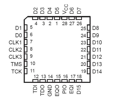
Pinout

  Connection Diagram


Specifications

Supply voltage range, VCC . . . . . . . . . . . . . . . . . . . . . . . . . . . . . . . . . . . . . . . . . . . . . . . . . . . . . . . 0.5 V to 7 V
Input voltage range, VI (see Note 1) . . . . . . . . . . . . . . . . . . . . . . . . . . . . . . . . . . . . . . . . . . . . . .  0.5 V to VCC
Output voltage range, VO (see Note 1) . . . . . . . . . . . . . . . . . . . . . . . . . . . . . . . . . . . . . . . . . . . . .0.5 V to VCC
Input clamp current, IIK (VI < 0 or VI > VCC) . . . . . . . . . . . . . . . . . . . . . . . . . . . . . . . . . . . . . . . . . . . . . .±20 mA
Output clamp current, IOK (VO < 0 or VO > VCC) . . . . . . . . . . . . . . . . . . . . . . . . . . . . . . . . . . . . . . . . . .  ±20 mA
Continuous output current, IO (VO = 0 to VCC) . . . . . . . . . . . . . . . . . . . . . . . . . . . . . . . . . . . . . . . . . . . . ±25 mA
Maximum power dissipation at TA = 55°C (in still air) (see Note 2) . . . . . . . . . . . . . . . . . . . . . . . . . . . . . . . 1.1 W
Storage temperature range, Tstg . . . . . . . . . . . . . . . . . . . . . . . . . . . . . . . . . . . . . . . . . . . . . . . . .65°C to 150°C
† Stresses beyond those listed under "absolute maximum ratings" may cause permanent damage to the device. These are stress ratings only, and
functional operation of the device at these or any other conditions beyond those indicated under "recommended operating conditions" is not
implied. Exposure to absolute-maximum-rated conditions for extended periods may affect device reliability.
NOTES: 1. The input and output voltage ratings may be exceeded if the input and output clamp-current ratings are observed.
2. The maximum package power dissipation is calculated using a junction temperature of 150°C and a board trace length of 75 mils.
For more information, refer to the Package Thermal Considerations application note in the ABT Advanced BiCMOS Technology Data
Book, literature number SCBD002.


Description

The SN74ACT8994 digital bus monitor (DBM) is a member of the Texas Instruments SCOPEE testability integrated-circuit family. This family of components supports IEEE Standard 1149.1-1990 (JTAG) boundary scan to facilitate testing of complex circuit-board assemblies. The DBM is a boundary-scannable device designed to monitor and/or store the values of a digital bus up to 16 bits in width. SN74ACT8994 resides in parallel with the bus being monitored.

Data at the D-input pins can be stored in a scannable random-access memory (RAM). Up to 1024 words of 16 bits can be stored. A parallel-signature analysis (PSA) can be performed on the data or on the contents of memory. The PSA operations use a linear-feedback shift-register technique to compress data into a signature. The user of SN74ACT8994 can configure the device to mask any combination of data inputs and control the feedback used during PSA operations.


Customers Who Bought This Item Also Bought

Margin,quality,low-cost products with low minimum orders. Secure your online payments with SeekIC Buyer Protection.
Optoelectronics
Computers, Office - Components, Accessories
Inductors, Coils, Chokes
Sensors, Transducers
Power Supplies - External/Internal (Off-Board)
View more