Features: EPIC(TM) (Enhanced-Performance Implanted
CMOS) Process
Operating Range 2-V to 5.5-V VCC
Latch-Up Performance Exceeds 250 mA Per
JESD 17
Package Options Include Plastic
Small-Outline Transistor (DBV, DCK)
Packages
Pinout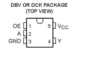 Specifications
Supply voltage range, V CC . . . . . . . . . . . . . . . . . . . . . . . . . . . . . . . . . . . . . . . . . . . . . . . . . . . . . . . . . . 0.5 V to 7 V
Output voltage range, VO (see Note 1) . . . . . . . . . . . . . . . . . . . . . . . . . . . . . . . . . . . . ........................... 0.5 V to 7V
Input clamp currentI IK (V I< 0) . . . . . . . . . . . . . . . . . . . . . . . . . . . . . . . . . . . . . . . . . . . . . . . . . . . . . . . . . . . 20 mA
Output clamp current, IOK (VO < 0 or VO > VCC ) . . . . . . . . . . . . . . . . . . . . . . . . . . . . . . . . . . . . . . . . . . . . ±20 mA
Continuous output current, IO (V CC = 0 to V CC) . . . . . . . . . . . . . . . . . . . . . . . . . . . . . . . . . . . . . . . . . . . . . ±25 mA
Continuous current through VCC or GND . . . . . . . . . . . . . . . . . . . . . . . . . . . . . . . . . . . . . . . . . . . . . . . . . . . ± 50 mA
Package thermal impedance, q JA (see Note 2): DBV package . . . . . . . . . . . . . . . . . . . . . . . . . . . . ........ . . 347°C/W
DCK package . . . . . . . . . . . . . . . . . . . . . . . . . . . . . . . 389°C/W
Storage temperature range, Tstg . . . . . . . . . . . . . . . . . . . . . . . . . . . . . . . . . . . . . . . . . . . . .. . . -65 °C to 150 ° C
DescriptionThe SN74AHC1G126 is a single bus buffer gate/line driver with 3-state output. The output is disabled when theoutput-enable (OE) input is low. When OE is high, true data is passed from the A input to the Y output.
To ensure the high-impedance state of SN74AHC1G126 during power up or power down, OE should be tied to GND through a pulldown resistor; the minimum value of the resistor is determined by the current-sourcing capability of the driver.
The SN74AHC1G126 is characterized for operation from 40°C to 85°C.

 SN74AHC1G126DBV Data Sheet


