Propagation Delay Time
:
Operating Temperature Range
:
Minimum Operating Temperature
: - 40 C
Packaging
: Reel
Maximum Operating Temperature
: + 85 C
Logic Type
: CMOS
Number of Circuits
: 1
Supply Voltage - Max
: 5.5 V
Logic Family
: 74AHC
Supply Voltage - Min
: 2 V
High Level Output Current
: - 8 mA
Low Level Output Current
: 8 mA
Package / Case
: SOT-23-5
Features: Operating Range of 2 V to 5.5 V
Max tpd of 8 ns at 5 V
Low Power Consumption, 10-µA Max ICC
±8-mA Output Drive at 5 V
Schmitt Trigger Action at All Inputs Makes the Circuit Tolerant for Slower Input Rise and Fall Time
Latch-Up Performance Exceeds 250 mA Per JESD 17Pinout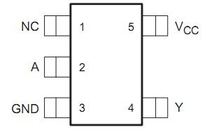 SpecificationsSupply voltage range, VCC . . . . . . . . . . . . . . . . . . . . . . . . . . . . . . −0.5 V to 7 V
Input voltage range, VI (see Note 1) . . . . . . . . . . . . . . . . . . . . . .−0.5 V to 7 V
Output voltage range, VO (see Note 1) . . . . . . . . . . . . . −0.5 V to VCC + 0.5 V
Input clamp current, IIK (VI < 0) . . . . . . . . . . . . . . . . . . . . . . . . . . . . . .−20 mA
Output clamp current, IOK (VO < 0 or VO > VCC) . . . . . . . . . . . . . . . . . .±20 mA
Continuous output current, IO (VO = 0 to VCC) . . . . . . . . . . . . . . . . . . .±25 mA
Continuous current through VCC or GND . . . . . . . . . . . . . . . . . . . . . . . .±50 mA
Package thermal impedance, JA (see Note 2): DBV package . . . . . .206°C/W
DCK package . . . . . .252°C/W
DRL package . . . . . .142°C/W
Storage temperature range, Tstg . . . . . . . . . . . . . . . . . . . . . . .−65°C to 150°C
† Stresses beyond those listed under "absolute maximum ratings" may cause permanent damage to the device. These are stress ratings only, and functional operation of the device at these or any other conditions beyond those indicated under "recommended operating conditions" is not implied. Exposure to absolute-maximum-rated conditions for extended periods may affect device reliability.
NOTES: 1. The input and output voltage ratings may be exceeded if the input and output current ratings are observed.
2. The package thermal impedance is calculated in accordance with JESD 51-7. DescriptionThis SN74LVC1G17 single Schmitt-trigger buffer is designed for 1.65-V to 5.5-V VCC operation.
The SN74LVC1G17 contains one buffer and performs the Boolean function Y = A. The device functions as an independent buffer, but because of Schmitt action, it may have different input threshold levels for positive-going (VT+) and negative-going (VT−) signals.
Parameters: | Technical/Catalog Information | SN74AHC1G14DBVR |
| Vendor | Texas Instruments (VA) |
| Category | Integrated Circuits (ICs) |
| Number of Circuits | 1 - Single |
| Package / Case | SOT-23-5 |
| Logic Type | Inverter with Schmitt Trigger |
| Packaging | Digi-Reel? |
| Mounting Type | Surface Mount |
| Number of Inputs | 1 |
| Current - Output High, Low | 8mA, 8mA |
| Supply Voltage | 2 V ~ 5.5 V |
| Operating Temperature | -40°C ~ 85°C |
| Voltage - Supply | 2 V ~ 5.5 V |
| Drawing Number | 296; 4073253-4; DBV; 5 |
| Lead Free Status | Lead Free |
| RoHS Status | RoHS Compliant |
| Other Names | SN74AHC1G14DBVR
SN74AHC1G14DBVR
296 1092 6 ND
29610926ND
296-1092-6
|

 SN74AHC1G14DBVR Data Sheet


