Switch Voltage (Max)
:
Switch Configuration
: SPST
Mounting Style
: SMD/SMT
Maximum Operating Temperature
: + 85 C
Number of Switches
: 4
Operating Supply Voltage
: 3 V, 5 V
Off Time (Max)
: 25 ns
On Time (Max)
: 25 ns
On Resistance (Max)
: 180 Ohms
Package / Case
: QFN-14
Features: ` 2-V to 5.5-V VCC Operation
` Supports Mixed-Mode Voltage Operation on All Ports
` High On-Off Output-Voltage Ratio
` Low Crosstalk Between Switches
` Individual Switch Controls
` Extremely Low Input Current
` ESD Protection Exceeds JESD 22
2000-V Human-Body Model (A114-A)
200-V Machine Model (A115-A)
1000-V Charged-Device Model (C101)Pinout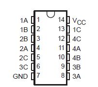 Specifications
Supply voltage range, VCC (see Note 1)...................................0.5 V to 7 V
Input voltage range, VI (see Note 1) .......................................0.5 V to 7 V
Switch I/O voltage range, VIO (see Notes 1 and 2) ......0.5 V to VCC + 0.5 V
Control-input clamp current, IIK (VI < 0) ............................................20 mA
I/O diode current, IIOK (VIO < 0 or VIO > VCC) ..................................±50 mA
On-state switch current, IT (VIO = 0 to VCC) ..................................... ±25 mA
Continuous current through VCC or GND .............................................±50 mA
Package thermal impedance, JA (see Note 3): D package ............... 86°C/W
(see Note 3): DB package ............. 96°C/W
(see Note 3): DGV package ..........127°C/W
(see Note 3): N package ................ 80°C/W
(see Note 3): NS package ...............76°C/W
(see Note 3): PW package ............ 113°C/W
(see Note 4): RGY package ............. 47°C/W
Storage temperature range, Tstg ..........................................65°C to 150°C
† Stresses beyond those listed under "absolute maximum ratings" may cause permanent damage to the device. These are stress ratings only, and functional operation of the device at these or any other conditions beyond those indicated under "recommended operating conditions" is not implied. Exposure to absolute-maximum-rated conditions for extended periods may affect device reliability.
NOTES: 1. The input and output voltage ratings may be exceeded if the input and output current ratings are observed.
2. This value is limited to 5.5 V maximum.
3. The package thermal impedance is calculated in accordance with JESD 51-7.
4. The package thermal impedance is calculated in accordance with JESD 51-5.
DescriptionThis SN74AHC4066RGYR quadruple silicon-gate CMOS analog switch is designed for 2-V to 5.5-V VCC operation.
This SN74AHC4066RGYR switch is designed to handle both analog and digital signals. Each switch permits signals with amplitudes up to 5.5 V (peak) to be transmitted in either direction.
Each SN74AHC4066RGYR switch section has its own enable-input control (C). A high-level voltage applied to C turns on the associated switch section.
Applications of SN74AHC4066RGYR include signal gating, chopping, modulation or demodulation (modem), and signal multiplexing for analog-to-digital and digital-to-analog conversion systems.
Parameters: | Technical/Catalog Information | SN74AHC4066RGYR |
| Vendor | Texas Instruments (VA) |
| Category | Integrated Circuits (ICs) |
| Type | Switch |
| Voltage Supply Source | Single Supply |
| Voltage - Supply, Single/Dual (±) | 2 V ~ 5.5 V |
| Circuit | 4 x 1:1 |
| On-State Resistance | 75 Ohm |
| Mounting Type | Surface Mount |
| Package / Case | 14-QFN |
| Packaging | Digi-Reel? |
| Current - Supply | - |
| Operating Temperature | -40°C ~ 85°C |
| Function | Switch |
| Drawing Number | 296; 4203539-2; RGY; 14 |
| Lead Free Status | Lead Free |
| RoHS Status | RoHS Compliant |
| Other Names | SN74AHC4066RGYR
SN74AHC4066RGYR
296 15258 6 ND
296152586ND
296-15258-6
|

 SN74AHC4066RGYR Data Sheet


