Features: Members of the Texas InstrumentsWidebusTM Family
EPICTM (Enhanced-Performance ImplantedCMOS) Process
Inputs Are TTL-Voltage Compatible
Distributed VCCand GND Pins MinimizeHigh-Speed Switching Noise
Flow-Through Architecture Optimizes PCBLayout
Latch-Up Performance Exceeds 250 mA PeJESD 17
Package Options Include Plastic Shrink
Small-Outline (DL), Thin Shrink
Small-Outline (DGG), and Thin Very
Small-Outline (DGV) Packages and 380-mil
Fine-Pitch Ceramic Flat (WD) Package
Using 25-mil Center-to-Center Spacings
Pinout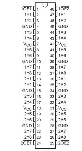 Specifications
Supply voltage range, VCC. . . . . . . . . . . . . . . . . . . . . .. . . . . . . . . . . . . . . . . . . . 0.5 V to 7 V
Input voltage range, VI (see Note 1) . . . . . . . . . . . . . . . . . . . . . . . . . . . . . . . 0.5 V to 7 V
Output voltage range, VO(see Note 1) . . . . . . . . . . . . . . . . . . . . . . . . . 0.5 V to VCC+ 0.5 V
Input clamp current, IIK (VI< 0) . . . . . . . . . . . . . . . . . . . . . . . . . . . . . . . . . . . . . . . . . 20 mA
Output clamp current, IOK(VO 0 or VO > VCC ) . . . . . . . . . . . . . . . . . . . . . . . . . . . . . ±20 mA
Continuous output current, IO (VO = 0 to VCC) . . . . . . . . . . . . . . . . . . . . . . . . . . . . . ±25 mA
Continuous current through each VCC or GND . . . . . . . . . . . . . . . . . . . . . . . . . . . . . ±75 mA
Package thermal impedance, JA (see Note 2): DGG package . . . . . . . . . . . . . .. . . . . . . 70/W
DGV package . . . . . . . . . . . . . . . . . . . . . 58/W
DL package . . . . . . . . . . . ...... . . . . . . . . 63/W
Storage temperature range, Tstg . . . . . . . . . . . . . . . . . . . . . . . . . . . . .. . . . . . . .65 to 150
DescriptionThe 'AHCT16541 devices are noninverting 16-bitbuffers composed of two 8-bit sections withseparate output-enable signals. For either 8-bitbuffer section, the two output-enable (1OE1 and1OE2 or 2OE1 and 2OE2) inputs must both be lowfor the corresponding Y outputs to be active. Ifeither output-enable input is high, the outputs ofthat 8-bit buffer section are in the high-impedancestate.
To ensure the high-impedance state of 'AHCT16541 during power up or power down, OE should be tied to VCC through a pullup resistor; the minimum value of the resistor is determined by the current-sinking capability of the driver.
The SN54AHCT16541 is characterized for operation over the full military temperature range of 55°C to 125°C.The SN74AHCT16541 is characterized for operation from 40°C to 85°C.

 SN74AHCT16541 Data Sheet


