Features: • 3-State Buffer-Type Outputs Drive Bus Lines Directly
• Bus-Structured Pinout
• Provides Extra Bus Driving Latches Necessary For Wider Address/Data Paths or Buses With Parity
• Buffered Control Inputs to Reduce DC Loading
• Power-Up High-Impedance State
• Package Options Include Plastic "Small Outline" Packages, Plastic Chip Carriers, and Standard Plastic 300-mil DIPs
• Dependable Texas Instruments Quality and Reliability
Pinout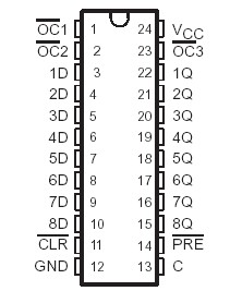 Specifications
Supply voltage, VCC (see Note 1) . . . . . . . . . . . . . . . . . . . . . . . . . . . . . . . . . . . . . . . . . . .7 V
Input voltage . . . . . . . . . . . . . . . . . . . . . . . . . . . . . . .. . . . . . . . . . . . . . . . . . . . . . . . . . . .7 V
Voltage applied to a disabled 3-state output . . . . . . . . . . . . . . . . . . . . . . . . . . . . . . . .5.5 V
Operating free-air temperature range . . . . . . . . . . . . . . .. . . . . . . . . . . . . . . . . .0°C to 70°C
Storage temperature range . . . . . . . . . . . . . . . . . . . . . . . . . . . . . . . . . . . . . 65°C to 150°C
DescriptionThese SN74ALS29845 8-bit latches feature three-state outputs designed specifically for driving highly capacitive or relatively low-impedance loads. SN74ALS29845 are particularly suitable for implementing buffer registers, I/O ports, bidirectional bus drivers, and working registers.
The SN74ALS29845 eight latches are transparent D-type. The 4ALS29845 has noninverting data (D) inputs. The 4ALS29846 has inverting D inputs. Since CLR and PRE are independent of the clock, taking the CLR input low will cause the eight Q outputs to go low. Taking the PRE input low will cause the eight Q outputs to go high. When both PRE and CLR are taken low, the outputs will follow the preset condition.
The buffered output control inputs of SN74ALS29845 (OC1, OC2, and OC3) can be used to place the eight outputs in either a normal logic state (high or low levels) or a high-impedance state. The outputs are also in the high-impedance state during power-up and power-down conditions. The outputs remain in the high-impedance state while the device is powered-down. In the high-impedance state, the outputs neither load nor drive the bus lines significantly. The high-impedance state and increased drive provide the capability to drive the bus lines in a bus-organized system without need for interface or pullup components. The output controls do not affect the internal operation of the latches. Old data can be retained or new data can be entered while the outputs are in the high-impedance state.
The SN74ALS29845 and SN74ALS29846 are characterized for operation from 0°C to 70°C

 SN74ALS29845 Data Sheet


