SN74ALVC16269

Features: EPICTM (Enhanced-Performance Implanted CMOS) Submicron ProcessMember of the Texas Instruments WidebusTM FamilyESD Protection Exceeds 2000 V Per MIL-STD-883C, Method 3015; Exceeds 200 V Using Machine Model (C = 200 pF, R = 0)Latch-Up Performance Exceeds 250 mA Per JEDEC Standard JESD-17Bu...

product image

SN74ALVC16269 Picture
SeekIC No. : 004498223 Detail

SN74ALVC16269: Features: EPICTM (Enhanced-Performance Implanted CMOS) Submicron ProcessMember of the Texas Instruments WidebusTM FamilyESD Protection Exceeds 2000 V Per MIL-STD-883C, Method 3015; Exceeds 200 V Usi...

floor Price/Ceiling Price

Part Number:
SN74ALVC16269
Supply Ability:
5000

Price Break

  • Qty
  • 1~5000
  • Unit Price
  • Negotiable
  • Processing time
  • 15 Days
Total Cost: $ 0.00

SeekIC Buyer Protection PLUS - newly updated for 2013!

  • Escrow Protection.
  • Guaranteed refunds.
  • Secure payments.
  • Learn more >>

Month Sales

268 Transactions

Rating

evaluate  (4.8 stars)

Upload time: 2025/12/25

Payment Methods

All payment methods are secure and covered by SeekIC Buyer Protection PLUS.

Notice: When you place an order, your payment is made to SeekIC and not to your seller. SeekIC only pays the seller after confirming you have received your order. We will also never share your payment details with your seller.
Product Details

Description


Features:

 EPICTM (Enhanced-Performance Implanted CMOS) Submicron Process
 Member of the Texas Instruments WidebusTM Family
 ESD Protection Exceeds 2000 V Per MIL-STD-883C, Method 3015; Exceeds 200 V Using Machine Model (C = 200 pF, R = 0)
 Latch-Up Performance Exceeds 250 mA Per JEDEC Standard JESD-17
 Bus Hold on Data Inputs Eliminates the Need for External Pullup/Pulldown Resistors
 Package Options Include Plastic Shrink Small-Outline (DL) and Thin Shrink Small-Outline (DGG) Packages


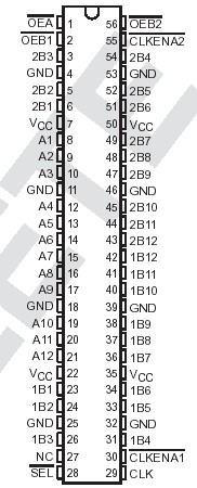
Pinout

  Connection Diagram


Specifications

Supply voltage range, VCC . . . . . . . . . . . . . . . . . . . . . . . . . . . . . . . . . . . . . . . . . . . . .0.5 V to 4.6 V
Input voltage range, VI: Except I/O ports (see Note 1) . . . . . . . . . . . . .. . . .   0.5 V to VCC + 4.6 V 
                                       (I/O ports) (see Notes 1 and 2). . . . . . . . . . . . . . . .   0.5 V to VCC + 0.5 V
Output voltage range, VO (see Notes 1 and 2) . . . . . . . . . . . . . . . . . . . . .  . . .0.5 V to VCC + 0.5 V
Input clamp current, IIK (VI < 0). . . . . . . . . . . . . . . . . . . . . . . . . . . . . . . . . . . . . . . . . . .. . . . 50 mA
Output clamp current, IOK (VO < 0 or VO > VCC) . . . . . . . . . . . . . . . . . . . . . . . . . . . . . . . . . . ±50 mA
Continuous output current, IO (VO = 0 to VCC) . . . . . . . . . . . . . . . . . . . . . . . . . . . . .. . . . . . .±50 mA
Continuous current through VCC or GND  . . . . . . . . . . . . . . . . . . . . . . . . . . . . . . . . . . . . . ... ±100mA
Maximum power package dissipation at TA = 55°C (in still air)(see Note 3):DGG package  . .  . .  1W
                                                                                                                     DL package . .  .   .1.4 W 
Storage temperature range ,Tstg . . .  . . . . . . . . . . . . . . . . . . . . . . . . . . . . . . .. . . . . .65°C to 150°C 


Description

The SN74ALVC16269 is a 12-bit to 24-bit registered bus transceiver, which is intended for applications where two separate ports must be multiplexed onto, or demultiplexed from, a single port. The device is particularly suitable as an interface between synchronous DRAMs and high-speed microprocessors. The SN74ALVC16269 is designed specifically for low-voltage (3.3-V) VCC operation; it is tested at 2.5-V, 2.7-V, and 3.3-V VCC.

Data is stored in the internal B-port registers on the low-to-high transition of the clock (CLK) input when the appropriate clock-enable (CLKENA) inputs are low. Proper control of these inputs allows two sequential 12-bit words to be presented as a 24-bit word on the B port. For data transfer in the B-to-A direction, a single storage register is provided. The select (SEL) line selects 1B or 2B data for the A outputs. The register on the A output permits the fastest possible data transfer, thus extending the period that the data is valid on the bus. The control terminals are registered so that all transactions are synchronous with CLK. Data flow is controlled by the active-low output enables (OEA, OEB1, OEB2).Active bus-hold circuitry is provided to hold unused or floating data inputs at a valid logic level.The SN74ALVC16269 is available in TI's shrink small-outline (DL) and thin shrink small-outline (DGG) packages, which provide twice the I/O pin count and functionality of standard small-outline packages in the same printed-circuit-board area.

The SN74ALVC16269 is characterized for operation from 40°C to 85°C.


Customers Who Bought This Item Also Bought

Margin,quality,low-cost products with low minimum orders. Secure your online payments with SeekIC Buyer Protection.
Discrete Semiconductor Products
Programmers, Development Systems
Isolators
Crystals and Oscillators
Optoelectronics
View more