Features: ` Member of the Texas Instruments WidebusTM Family
` EPICTM (Enhanced-Performance Implanted CMOS) Submicron Process
` Output Ports Have Equivalent 26- Series Resistors, So No External Resistors Are Required
` ESD Protection Exceeds 2000 V Per MIL-STD-883, Method 3015; Exceeds 200 V Using Machine Model (C = 200 pF, R = 0)
` Latch-Up Performance Exceeds 250 mA Per JESD 17
` Packaged in Thin Very Small-Outline PackagePinout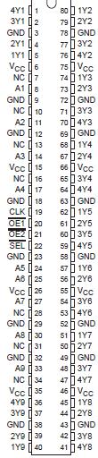 Specifications
Supply voltage range, VCC . . . . . . . . . . . . . . . . . . . . . . . . . . . . . . . . . . . . . . . . . . 0.5 V to 4.6 V
Input voltage range, VI (see Note 1) . . . . . . . . . . . . . . . . . . . . . . . . . . . . . . . . . . 0.5 V to 4.6 V
Output voltage range, VO (see Notes 1 and 2) . . . . . . . . . . . . . . . . . . . . . 0.5 V to VCC + 0.5 V
Input clamp current, IIK (VI < 0) . . . . . . . . . . . . . . . . . . . . . . . . . . . . . . . . . . . . . . . . . . . . 50 mA
Output clamp current, IOK (VO < 0) . . . . . . . . . . . . . . . . . . . . . . . . . . . . . . . . .. . . . . . . . . 50 mA
Continuous output current, IO . . . . . . . . . . . . . . . . . . . . . . . . . . . . . . . . . . . . . . . . . . . . . ±50 mA
Continuous current through each VCC or GND . . . . . . . . . . . . . . . . . . . . . . . . . . . . .. . . . ±100 mA
Package thermal impedance, JA (see Note 3) . . . . . . . . . . . . . . . . . . . . . . . . . . . . . . . . 106°C/W
Storage temperature range, Tstg . . . . . . . . . . . . . . . . . . . . . . . . . . . . . . . . . .. . 65°C to 150°C
† Stresses beyond those listed under "absolute maximum ratings" may cause permanent damage to the device. These are stress ratings only, and functional operation of the device at these or any other conditions beyond those indicated under "recommended operating conditions" is not implied. Exposure to absolute-maximum-rated conditions for extended periods may affect device reliability.
NOTES: 1. The input negative-voltage and output voltage ratings may be exceeded if the input and output current ratings are observed.
2. This value is limited to 4.6 V maximum.
3. The package thermal impedance is calculated in accordance with JESD 51.
DescriptionThis SN74ALVC162831 1-bit to 4-bit address register/driver is designed for 1.65-V to 3.6-V VCC operation.
The SN74ALVC162831 is ideal for use in applications in which a single address bus is driving four separate memory locations. The SN74ALVC162831 can be used as a buffer or a register, depending on the logic level of the select (SEL) input. When SEL is logic high, the device is in the buffer mode. The outputs follow the inputs and are controlled by the two output-enable (OE) inputs. Each OE controls two groups of nine outputs.When SEL is logic low, the device is in the register mode. The register is an edge-triggered D-type flip-flop. On the positive transition of the clock (CLK) input, data set up at the A inputs is stored in the internal registers. OE controls operate the same as in buffer mode.When OE is logic low, the outputs are in a normal logic state (high or low logic level). When OE is logic high, the outputs are in the high-impedance state. SEL and OE do not affect the internal operation of the flip-flops. Old data can be retained or new data can be entered while the outputs are in the high-impedance state.

 SN74ALVC162831 Data Sheet


