Features: Member of the Texas Instruments Widebus+TM Family
UBETMUBTE (Universal Bus Transceiver) Combines D-Type Latches and D-Type Flip-Flops for Operation in Transparent, Latched, Clocked, or Clock-Enabled Mode
• EPICTM (Enhanced-Performance Implanted CMOS) Submicron Process
Designed to Facilitate Incident-Wave Switching for Line Impedances of 50 W or Greater
Typical VOLP (Output Ground Bounce) < 0.8 V at VCC = 3.3 V, TA = 25°C
Typical VOHV (Output VOH Undershoot) > 2 V at VCC = 3.3 V, TA = 25°C
Bus Hold on Data Inputs Eliminates the Need for External Pullup/Pulldown Resistors
Package Options Include Plastic 300-mil Shrink Small-Outline (DL) and Thin Shrink Small-Outline (DGG) Packages
Pinout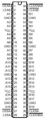 SpecificationsSupply voltage range, VCC . . . . . . . . . . . . . . . . . . . . . . . . . . . . . . . . . . . . . . . . . . . . .0.5 V to 4.6 V
Input voltage range, VI: (except I/O ports) (see Note 1) . . . . . . . . . . . .. . . . . . . . ..0.5 V to 4.6 V
Input voltage range, VI:(I/O ports) (see Notes 1 and 2). . . . . . . . . . . . . . . . 0.5 V to VCC + 0.5 V
Output voltage range, VO (see Notes 1 and 2) . . . . . . . . . . . . . . . . . . . . . . . .0.5 V to VCC + 0.5 V
Input clamp current, IIK (VI < 0). . . . . . . . . . . . . . . . . . . . . . . . . . . . . . . . . . . . . . . . . . .. . . . 50 mA
Output clamp current, IOK (VO < 0 or VO > VCC) . . . . . . . . . . . . . . . . . . . . . . . . . . . . . . . . . . ±50 mA
Continuous output current, IO (VO = 0 to VCC) . . . . . . . . . . . . . . . . . . . . . . . . . . . . .. . . . . . .±50 mA
Continuous current through VCC or GND . . . . . . . . . . . . . . . . . . . . . . . . . . . . . . . . . . . . . ... ±100mA
Maximum power package dissipation at TA = 55°C (in still air)(see Note 3):DGG package . . . . 1 W
DL package . .. . . . 1.4 W
Storage temperature range . . . . . . . . . . . . . . . . . . . . . . . . . . . . . . . . . . . . .. . . . . .65°C to 150°C DescriptionThis 18-bit universal bus transceiver is designed for 2.7-V to 3.6-V VCC operation.The SN74ALVC16600 combines D-type latches and D-type flip-flops to allow data flow in transparent, latched, and clocked modes.
Data flow in each direction is controlled by output-enable (OEAB and OEBA), latch-enable (LEAB and LEBA), and clock (CLKAB and CLKBA) inputs. The clock can be controlled by the clock-enable (CLKENAB and CLKENBA) inputs. For A-to-B data flow, the device operates in the transparent mode when LEAB is high. When LEAB is low, the A data is latched if CLKAB is held at a high or low logic level. If LEAB is low, the A-bus data is stored in the latch/flip-flop on the high-to-low transition of CLKAB. Output enable OEAB is active low. When OEAB is low, the outputs are active. When OEAB is high, the outputs are in the high-impedance state.
Data flow for B to A is similar to that of A to B but uses OEBA, LEBA, CLKBA, and CLKENBA.The SN74ALVC16600 is available in TI's shrink small-outline (DL) and thin shrink small-outline (DGG) packages, which provide twice the I/O pin count and functionality of standard small-outline packages in the same printed-circuit-board area.
The SN74ALVC16600 is characterized for operation from 40°C to 85°C.

 SN74ALVC16600 Data Sheet


