Features: Member of the Texas Instruments
Widebus Family
EPIC (Enhanced-Performance Implanted
CMOS) Submicron Process
ESD Protection Exceeds 2000 V Per
MIL-STD-883, Method 3015; Exceeds 200 V
Using Machine Model (C = 200 pF, R = 0)
Latch-Up Performance Exceeds 250 mA Per
JESD 17
Bus Hold on Data Inputs Eliminates the
Need for External Pullup/Pulldown
Resistors
Package Options Include Plastic Shrink
Small-Outline (DL) and Thin Shrink
Small-Outline (DGG) PackagesPinout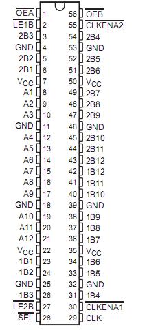 SpecificationsSupply voltage range, VCC . . . . . . . . . . . . . . . . . . . . . . . . . . . . . . . . . . . . . . . . . . . . . . . . . . . . 0.5 V to 4.6 V
Input voltage range, VI: Except I/O ports (see Note 1) . . . . . . . . . . . . . . . . . . . . . . . . . . . . . .0.5 V to 4.6 V
I/O ports (see Notes 1 and 2) . . . . . . . . . . . . . . . . . . . . . . . . 0.5 V to VCC + 0.5 V
Output voltage range, VO (see Notes 1 and 2) . . . . . . . . . . . . . . . . . . . . . . . . . . . . . . .0.5 V to VCC + 0.5 V
Input clamp current, IIK (VI < 0) . . . . . . . . . . . . . . . . . . . . . . . . . . . . . . . . . . . . . . . . . . . . . . . . . . . . . 50 mA
Output clamp current, IOK (VO < 0) . . . . . . . . . . . . . . . . . . . . . . . . . . . . . . . . . . . . . . . . . . . . . . . . . . 50 mA
Continuous output current, IO . . . . . . . . . . . . . . . . . . . . . . . . . . . . . . . . . . . . . . . . . . . . . . . . . . . . . . . ±50 mA
Continuous current through each VCC or GND . . . . . . . . . . . . . . . . . . . . . . . . . . . . . . . . . . . . . . . . . . .±100mA
Package thermal impedance, JA (see Note 3): DGG package . . . . . . . . . . . . . . . . . . . . . . . . . . . . . . . 81°C/W
DL package . . . . . . . . . . . . . . . . . . . . . . . . . . . . . . . . .74°C/W
Storage temperature range, Tstg . . . . . . . . . . . . . . . . . . . . . . . . . . . . . . . . . . . . . . . . . . . . . 65°C to 150°C
Stresses beyond those listed under "absolute maximum ratings" may cause permanent damage to the device. These are stress ratings only, and functional operation of the device at these or any other conditions beyond those indicated under "recommended operating conditions" is not implied. Exposure to absolute-maximum-rated conditions for extended periods may affect device reliability.
NOTES:
1. The input negative-voltage and output voltage ratings may be exceeded if the input and output current ratings are observed.
2. This value is limited to 4.6 V maximum.
3. The package thermal impedance is calculated in accordance with JESD 51. DescriptionThis SN74ALVCH16271 12-bit to 24-bit bus exchanger is designed for 1.65-V to 3.6-V V
CC operation.
The SN74ALVCH16271 is intended for applications in which two separate data paths must be multiplexed onto, or demultiplexed from,a single data path. This device is particularly suitable as an interface between conventional DRAMs and high-speed microprocessors.
A data is stored in the internal A-to-B registers on the low-to-high transition of the clock (CLK) input, provided that the clock-enable (,CLKENA) inputs are low. Proper control of these inputs allows two sequential 12-bit words to be presented as a 24-bit word on the B port. Transparent latches in the B-to-A path allow asynchronous operation to maximize memory access throughput. These latches transfer data when the latch-enable (,LE) inputs are low. The select (,SEL) line selects 1B or 2B data for the A outputs. Data flow is controlled by the active-low output enables (,OEA ,OEB).To ensure the high-impedance state of SN74ALVCH16271 during power up or power down, the output enables should be tied to V
CC through a pullup resistor; the minimum value of the resistor is determined by the current-sinking capability of the driver.Active bus-hold circuitry is provided to hold unused or floating data inputs at a valid logic level.
The SN74ALVCH16271 is characterized for operation from 40°C to 85°C.

 SN74ALVCH16271 Data Sheet


