Features: · Member of the Texas Instruments Widebus+TM Family
· EPICTM (Enhanced-Performance Implanted CMOS) Submicron Process
· UBE E (Universal Bus Exchanger) Allows Synchronous Data Exchange
· ESD Protection Exceeds 2000 V Per MIL-STD-883, Method 3015; Exceeds 200 V Using Machine Model (C = 200 pF, R = 0)
· Latch-Up Performance Exceeds 250 mA Per JESD 17
· Bus Hold on Data Inputs Eliminates the Need for External Pullup/Pulldown Resistors
· Package Options Include Plastic 300-mil Shrink Small-Outline (DL) and Thin Shrink Small-Outline (DGG) Packages
Pinout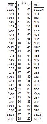 Specifications
Supply voltage range, VCC . . . . . . . . . . . . . . . . . . . . . . . . . . . . . . . . . . . . . .. . . 0.5 V to 4.6 V
Input voltage range, VI: Except I/O ports (see Note 1) . . . . . . . . . . .. . . . . . . . 0.5 V to 4.6 V
I/O ports (see Notes 1 and 2) . . . . . . . . . . . . . 0.5 V to VCC + 0.5 V
Output voltage range, VO (see Notes 1 and 2) . . . . . . . . . . . . . . . . .. . . 0.5 V to VCC + 0.5 V
Input clamp current, IIK (VI < 0) . . . . . . . . . . . . . . . . . . . . . . . . . . . . . . . . . . . . . . . . . . 50 mA
Output clamp current, IOK (VO < 0) . . . . . . . . . . . . . . . . . . . . . . . . . . . . . . . . .. . . . . . . 50 mA
Continuous output current, IO . . . . . . . . . . . . . . . . . . . . . . . . . . . . . . . . . . . . .. . . . . . . ±50 mA
Continuous current through each VCC or GND . . . . . . . . . . . . . . . . . . . . . . . . . . . . . . ±100 mA
Package thermal impedance, JA (see Note 3): DGG package . . . . . . . . . . . . . . . . . . . 81°C/W
DL package . . . . . . . . . . . . . . . . . . . . 74°C/W
Storage temperature range, Tstg . . . . . . . . . . . . . . . . . . . . . . . . . . . . . . . . . 65°C to 150°C
† Stresses beyond those listed under "absolute maximum ratings" may cause permanent damage to the device. These are stress ratings only, and functional operation of the device at these or any other conditions beyond those indicated under "recommended operating conditions" is not implied. Exposure to absolute-maximum-rated conditions for extended periods may affect device reliability.
NOTES: 1. The input negative-voltage and output voltage ratings may be exceeded if the input and output current ratings are observed.
2. This value is limited to 4.6 V maximum.
3. The package thermal impedance is calculated in accordance with JESD 51.
DescriptionThis SN74ALVCH16409 9-bit, 4-port universal bus exchanger is designed for 1.65-V to 3.6-V VCC operation.
The SN74ALVCH16409 allows synchronous data exchange between four different buses. Data flow is controlled by the select (SEL0SEL4) inputs. A data-flow state is stored on the rising edge of the clock (CLK) input if the select-enable (SELEN) input is low. Once a data-flow state has been established, data is stored in the flip-flop on the rising edge of CLK if SELEN is high. The data-flow control logic is designed to allow glitch-free data transmission.
When preset (PRE) transitions high, the outputs are disabled immediately, without waiting for a clock pulse. To leave the high impedance state, both PRE and SELEN must be low and a clock pulse must be applied. To ensure the high-impedance state of SN74ALVCH16409 during power up or power down, PRE should be tied to VCC through a pullup resistor; the minimum value of the resistor is determined by the current-sinking capability of the driver.
Active bus-hold circuitry is provided to hold unused or floating data inputs at a valid logic level.The SN74ALVCH16409 is characterized for operation from 40°C to 85°C.

 SN74ALVCH16409 Data Sheet


