Features: ` State-of-the-Art Advanced BiCMOS Technology (ABT) WidebusTM Design for 2.5-V and 3.3-V Operation and Low Static Power Dissipation
` Support Mixed-Mode Signal Operation (5-V Input and Output Voltages With 2.3-V to 3.6-V VCC)
` Typical VOLP (Output Ground Bounce) <0.8 V at VCC = 3.3 V, TA = 25°C
` High Drive (24/24 mA at 2.5-V and 32/64 mA at 3.3-V VCC)
` Power Off Disables Outputs, Permitting Live Insertion
` High-Impedance State During Power Up and Power Down Prevents Driver Conflict
` Use Bus Hold on Data Inputs in Place of External Pullup/Pulldown Resistors to Prevent the Bus From Floating
` Auto3-State Eliminates Bus Current Loading When Output Exceeds VCC + 0.5 V
` Latch-Up Performance Exceeds 250 mA Per JESD 17
` ESD Protection Exceeds 2000 V Per MIL-STD-883, Method 3015; Exceeds 200 V Using Machine Model; and Exceeds 1000 V Using Charged-Device Model, Robotic Method
` Flow-Through Architecture Facilitates Printed Circuit Board Layout
` Distributed VCC and GND Pin Configuration Minimizes High-Speed Switching Noise
` Package Options Include Plastic Shrink Small-Outline (DL), Thin Shrink Small-Outline (DGG), Thin Very Small-Outline (DGV) Packages, and 380-mil Fine-Pitch Ceramic Flat (WD) Package
Pinout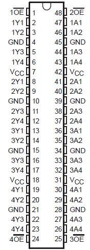 Specifications
Supply voltage range, VCC . . . . . . . . . . . . . . . . . . . . . . . . . . . . . . . . . . . . . . . . . . . . . 0.5 V to 4.6 V
Input voltage range, VI (see Note 1) . . . . . . . . . . . . . . . . . . . . . . . . . . . . . . .. . . . . . . . 0.5 V to 7 V
Voltage range applied to any output in the high-impedance
or power-off state, VO (see Note 1) . . . . . . . . . . . . . . . . . . . . . . . . . . . . . . . . . . . . . . 0.5 V to 7 V
Voltage range applied to any output in the high state, VO (see Note 1) . . . . . . . . . . . . 0.5 V to 7 V
Output current in the low state, IO: SN54ALVTH16240 . . . . . . . . . . . . . . . . . . . . . . . . . . . . . . . 96 mA
SN74ALVTH16240 . . . . . . . . . . . . . . . . . . . . . . . . . . . . . . 128 mA
Output current in the high state, IO: SN54ALVTH16240 . . . . . . . . . . . . . . . . . . . . . . . . . . . . . 48 mA
SN74ALVTH16240 . . . . . . . . . . . . . . . . . . . . . . . . . . . . . 64 mA
Input clamp current, IIK (VI < 0) . . . . . . . . . . . . . . . . . . . . . . . . . . . . . . . . . . . . . . . . . . . . . . .50 mA
Output clamp current, IOK (VO < 0) . . . . . . . . . . . . . . . . . . . . . . . . . . . . . . . . . . .. . . . . . . . . .. 50 mA
Package thermal impedance, JA (see Note 2): DGG package . . . . . . . . . . . . . . . . . . . . . . . 89°C/W
DGV package . . . . . . . . . . . . . . . . . . . . . . . . 93°C/W
DL package . . . . . . . . . . . . . . . . . . . . . . . . . . 94°C/W
Storage temperature range, Tstg . . . . . . . . . . . . . . . . . . . . . . . . . . . . . . . .. . . . . . . 65°C to 150°C
† Stresses beyond those listed under "absolute maximum ratings" may cause permanent damage to the device. These are stress ratings only, and functional operation of the device at these or any other conditions beyond those indicated under "recommended operating conditions" is not implied. Exposure to absolute-maximum-rated conditions for extended periods may affect device reliability.
NOTES: 1. The input and output negative-voltage ratings may be exceeded if the input and output clamp-current ratings are observed.
2. The package thermal impedance is calculated in accordance with JESD 51.
DescriptionThe SN74ALVTH16240 devices are 16-bit buffers/line drivers designed for 2.5-V or 3.3-V VCC operation, but with the capability to provide a TTL interface to a 5-V system environment.
These SN74ALVTH16240 devices are designed specifically to improve both the performance and density of 3-state memory address drivers, clock drivers, and bus-oriented receivers and transmitters.

 SN74ALVTH16240 Data Sheet


