Features: State-of-the-Art Advanced BiCMOS Technology (ABT) WidebusTM Design for 2.5-V and 3.3-V Operation and Low Static-Power Dissipation
Support Mixed-Mode Signal Operation (5-V Input and Output Voltages With 2.3-V to 3.6-V VCC)
Typical VOLP (Output Ground Bounce) <0.8 V at VCC = 3.3 V, TA = 25°C
High-Drive (24 mA/24 mA at 2.5-V and 32/64mA at 3.3-V VCC)
Ioff and Power-Up 3-State Support Hot Insertion
Use Bus Hold on Data Inputs in Place of External Pullup/Pulldown Resistors to Prevent the Bus From Floating
Auto3-State Eliminates Bus Current Loading When Output Exceeds VCC + 0.5 V
Flow-Through Architecture Facilitates Printed Circuit Board Layout
Distributed VCC and GND Pins Minimize High-Speed Switching Noise
Package Options Include Plastic 300-mil Shrink Small-Outline (DL), Thin Shrink Small-Outline (DGG), Thin Very Small-Outline (DGV) Packages, and 380-mil Fine-Pitch Ceramic Flat (WD) Package
Pinout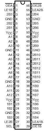 SpecificationsSupply voltage range, VCC . . . . . . . . . . . . . . . . . . . . . . . . . . . . . . . . . . . . . . . .. .0.5 V to 4.6 V
Input voltage range, VI (see Note 1). . . . . . . . . . . . . . . . . . . . . . . . . . . . . . . . . . . . 0.5 V to 7 V
Voltage range applied to any output in the high-impedance
or power-off state, VO (see Note 1) . . . . . . . . . . . . . . . . . . . . . . . . . . . . . .. . . . .0.5 V to 7 V
Voltage range applied to any output in the high state, VO (see Note 1) . . . . . . . . .0.5 V to 7 V
Output current in the low state, IO: SN54ALVTH16260 . . . . . . . . . . . . . . . . . . . . . . . . . . .96 mA
SN74ALVTH16260 . . . . . . . . . . . . . . . . . . . . . . . . . .128 mA
Output current in the high state, IO: SN54ALVTH16260 . . . . . . . . . . . .. . . . . . . . . . . . . . . 48 mA
SN74ALVTH16260 . . . . . . . . . . . . . . . . . . . . . . . . . .64 mA
Continuous current through VCC or GND . . . . . . . . . . . . . . . . . . . . . .. . . . . . . . . . . . .. . .±100 mA
Input clamp current, IIK (VI < 0) . . . . . . . . . . . . . . . . . . . . . . . . . . . . . . . . . . . . . . . . . . . .50 mA
Output clamp current, IOK (VO < 0) . . . . . . . . . . . . . . . . . . . . . . . . . . . . . . . . . . . . . . . . . . 50 mA
Package thermal impedance, JA (see Note 2) DGG package . . . . . . . . . . . . . . . . . . . . . .64°C/W
DGV package . . . . . . . . . . . . . . . . . . . . . ..48°C/W
DL package . . . . . . . . . . . . . . . . . . . . .. . . 56°C/W
Storage temperature range, Tstg . . . . . . . . . . . . . . . . . . . .. . . . . . . . . . . . . . . . . ..65°C to 150°C DescriptionThe SN74ALVTH16260 devices are 12-bit to 24-bit multiplexed D-type latches designed for 2.5-V or 3.3-V VCC operation, but with the capability to provide a TTL interface to a 5-V system environment.
Three 12-bit I/O ports (A1A12, 1B11B12, and 2B12B12) are available for address and/or data transfer. The output-enable (OE1B, OE2B, and OEA) inputs control the bus transceiver functions. The OE1B and OE2B control signals also allow bank control in the A-to-B direction. The SN74ALVTH16260 devices are used in applications where two separate data paths must be multiplexed onto, or demultiplexed from, a single data path. Typical applications include multiplexing and/or demultiplexing address and data information in microprocessor or bus-interface applications. This device also is useful in memory-interleaving applications.
Address and/or data information can be stored using the internal storage latches. The latch-enable (LE1B, LE2B, LEA1B, and LEA2B) inputs control data storage. When the latch-enable input is high, the latch is transparent. When the latch-enable input goes low, the data present at the inputs is latched and remains latched until the latch-enable input is returned high. These SN74ALVTH16260 devices are fully specified for hot-insertion applications using Ioff and power-up 3-state. The Ioff circuitry disables the outputs, preventing damaging current backflow through the device when it is powered down. The power-up 3-state circuitry places the outputs in the high-impedance state during power up and power down, which prevents driver conflict.
When VCC is between 0 and 1.2 V, the device is in the high-impedance state during power up or power down. However, to ensure the high-impedance state above 1.2 V, OE should be tied to VCC through a pullup resistor; the minimum value of the resistor is determined by the current-sinking capability of the driver.Active bus-hold circuitry is provided to hold unused or floating data inputs at a valid logic level.he SN54ALVTH16260 is characterized for operation over the full military temperature range of 55°C to 125°C. The SN74ALVTH16260 is characterized for operation from 40°C to 85°C.

 SN74ALVTH16260 Data Sheet


