Features: · State-of-the-Art Advanced BiCMOS Technology (ABT) WidebusE Design for 2.5-V and 3.3-V Operation and Low Static Power Dissipation
· Support Mixed-Mode Signal Operation (5-V Input and Output Voltages With 2.3-V to 3.6-V VCC)
·Typical VOLP (Output Ground Bounce) <0.8 V at VCC = 3.3 V, TA = 25°C
· Power Off Disables Outputs, Permitting Live Insertion
· High-Impedance State During Power Up and Power Down Prevents Driver Conflict
· Uses Bus Hold on Data Inputs in Place of External Pullup/Pulldown Resistors to Prevent the Bus From Floating
· Output Ports Have Equivalent 30-W Series Resistors, So No External Resistors Are Required
· Auto3-State Eliminates Bus Current Loading When Output Exceeds VCC + 0.5 V
· Latch-Up Performance Exceeds 250 mA Per JESD 17
· ESD Protection Exceeds 2000 V Per MIL-STD-883, Method 3015; Exceeds 200 V Using Machine Model; and Exceeds 1000 V Using Charged-Device Model, Robotic Method
· Flow-Through Architecture Facilitates Printed Circuit Board Layout
· Distributed VCC and GND Pin Configuration Minimizes High-Speed Switching Noise
· Package Options Include Plastic Shrink Small-Outline (DL), Thin Shrink Small-Outline (DGG), Thin Very Small-Outline (DGV) Packages, and 380-mil Fine-Pitch Ceramic Flat (WD) PackagePinout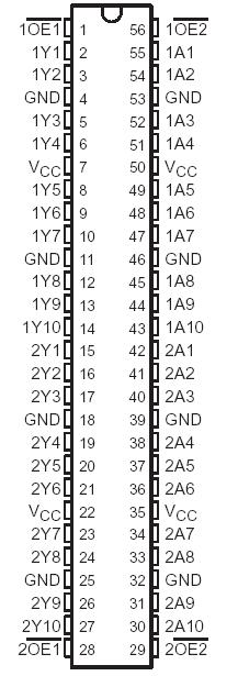 SpecificationsSupply voltage range, . . . . . . . . . . . . . . . . . . . . . . . . . . . . . . . . . . . .VCC 0.5 V to 4.6 V
Input voltage range, VI (see Note 1) . . . . . . . . . . . . . . . . . . . . . . . . . . . . . 0.5 V to 7 V
Voltage range applied to any output in the high-impedance
or power-off state, VO (see Note 1) . . . . . . . . . . . . . . . . . . . . . . . . . . . . . . 0.5 V to 7 V
Voltage range applied to any output in the high state, VO (see Note 1) . . 0.5 V to 7 V
Output current in the low state, IO: SN54ALVTH162827 . . . . . . . . . . . . . . . . . . . . 96 mA
SN74ALVTH162827 . . . . . . . . . . . . . . . . . . . . . . . . . . . . . . . . . . . . . . . . . . . . . . . 128 mA
Output current in the high state, IO: SN54ALVTH162827 . . . . . . . . . . . . . . . . . . 48 mA
SN74ALVTH162827 . . . . . . . . . . . . . . . . . . . . . . . . . . . . . . . . . . . . . . . . . . . . . . . 64 mA
Input clamp current, . . . . . . . . . . . . . . . . . . . . . . . . . . . . . . . . . . . . . .IIK (VI < 0) 50 mA
Output clamp current, . . . . . . . . . . . . . . . . . . . . . . . . . . . . . . . . . . . .IOK (VO < 0) 50 mA
Package thermal impedance, JA (see Note 2): DGG package . . . . . . . . . . . . . . .81°C/W
DGV package . . . . . . . . . . . . . . . . . . . . . . . . . . . . . . . . . . . . . . . . . . . . . . . . . . . . 86°C/W
DL package . . . . . . . . . . . . . . . . . . . . . . . . . . . . . . . . . . . . . . . . . . . . . . . . . . . . . 74°C/W
Storage temperature range, Tstg . . . . . . . . . . . . . . . . . . . . . . . . . . . . . 65°C to 150°C
Stresses beyond those listed under "absolute maximum ratings" may cause permanent damage to the device. These are stress ratings only, and functional operation of the device at these or any other conditions beyond those indicated under "recommended operating conditions" is not implied. Exposure to absolute-maximum-rated conditions for extended periods may affect device reliability.
NOTES: 1. The input and output negative-voltage ratings may be exceeded if the input and output clamp-current ratings are observed.
2. The package thermal impedance is calculated in accordance with JESD 51.
DescriptionThe SN74ALVTH162827 devices are composed of two 10-bit sections with separate output-enable signals. For either 10-bit buffer section, the two output-enable (1OE1 and 1OE2, or 2OE1 and 2OE2) inputs must be low for the corresponding Y outputs to be active. If either output-enable input is high, the outputs of that 10-bit buffer section are in the high-impedance state.
When VCC of SN74ALVTH162827 is between 0 and 1.2 V, the device is in the high-impedance state during power up or power down. However, to ensure the high-impedance state above 1.2 V, OE should be tied to VCC through a pullup resistor; the minimum value of the resistor is determined by the current-sinking capability of the driver.
All outputs of SN74ALVTH162827 are designed to sink up to 12 mA, and include equivalent 30-W resistors to reduce overshoot and undershoot. Active bus-hold circuitry is provided to hold unused or floating data inputs at a valid logic level.
The SN54ALVTH162827 is characterized for operation over the full military temperature range of 55°C to 125°C. The SN74ALVTH162827 is characterized for operation from 40°C to 85°C.

 SN74ALVTH162827 Data Sheet


