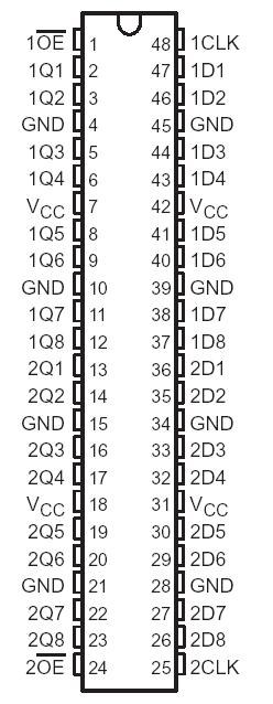
SN74ALVTH16374

Features: ` State-of-the-Art Advanced BiCMOS Technology (ABT) WidebusE Design for 2.5-V and 3.3-V Operation and Low StaticPower Dissipation` Support Mixed-Mode Signal Operation (5-V Input and Output Voltages With 2.3-V to 3.6-V VCC)`Typical VOLP (Output Ground Bounce) < 0.8 V at VCC = 3.3 V, TA...

product image

SN74ALVTH16374 Picture
SeekIC No. : 004498336 Detail

SN74ALVTH16374: Features: ` State-of-the-Art Advanced BiCMOS Technology (ABT) WidebusE Design for 2.5-V and 3.3-V Operation and Low StaticPower Dissipation` Support Mixed-Mode Signal Operation (5-V Input and Output...

floor Price/Ceiling Price

Part Number:
SN74ALVTH16374
Supply Ability:
5000

Price Break

  • Qty
  • 1~5000
  • Unit Price
  • Negotiable
  • Processing time
  • 15 Days
Total Cost: $ 0.00

SeekIC Buyer Protection PLUS - newly updated for 2013!

  • Escrow Protection.
  • Guaranteed refunds.
  • Secure payments.
  • Learn more >>

Month Sales

268 Transactions

Rating

evaluate  (4.8 stars)

Upload time: 2025/12/24

Payment Methods

All payment methods are secure and covered by SeekIC Buyer Protection PLUS.

Notice: When you place an order, your payment is made to SeekIC and not to your seller. SeekIC only pays the seller after confirming you have received your order. We will also never share your payment details with your seller.
Product Details

Description


Features:

` State-of-the-Art Advanced BiCMOS Technology (ABT) WidebusE Design for 2.5-V and 3.3-V Operation and Low Static
Power Dissipation
` Support Mixed-Mode Signal Operation (5-V Input and Output Voltages With 2.3-V to 3.6-V VCC)
`Typical VOLP (Output Ground Bounce) < 0.8 V at VCC = 3.3 V, TA = 25°C
`High Drive (24/24 mA at 2.5-V and 32/64 mA at 3.3-V VCC)
` Power Off Disables Outputs, Permitting Live Insertion
` High-Impedance State During Power Up and Power Down Prevents Driver Conflict
` Uses Bus Hold on Data Inputs in Place of
-External Pullup/Pulldown Resistors to
-Prevent the Bus From Floating
` Auto3-State Eliminates Bus Current
-Loading When Output Exceeds VCC + 0.5 V
` Latch-Up Performance Exceeds 250 mA Per JESD 17
` ESD Protection Exceeds 2000 V Per
-MIL-STD-883, Method 3015; Exceeds 200 V
-Using Machine Model; and Exceeds 1000 V
-Using Charged-Device Model, Robotic
-Method
` Flow-Through Architecture Facilitates
-Printed Circuit Board Layout
` Distributed VCC and GND Pin Configuration
-Minimizes High-Speed Switching Noise
` Package Options Include Plastic Shrink
-Small-Outline (DL), Thin Shrink
-Small-Outline (DGG), Thin Very
-Small-Outline (DGV) Packages, and 380-mil
-Fine-Pitch Ceramic Flat (WD) Package


Pinout

  Connection Diagram


Specifications

Supply voltage range, VCC . . . . . . . . . . . . . . . .. . . . . . . . . . . . . . . . . . . .0.5 V to 4.6 V
Input voltage range, VI (see Note 1) . . . . . .. . . . . . . . . . . . . . . . . . . . . . . .0.5 V to 7 V
Voltage range applied to any output in the high-impedance
or power-off state, VO (see Note 1) . . . . . . . . . . . . . . . . . . . . . . . . . . . . . .0.5 V to 7 V
Voltage range applied to any output in the high state, VO (see Note 1) . .0.5 V to 7 V
Output current in the low state, IO: SN54ALVTH16374 . . . . . . . . . . . . . . . . . . . . . 96 mA
SN74ALVTH16374 . . . . . . . . . . . . . . . . . . . . . . . . . . . . . . . . . . . . . . . . . . . . . . . . 128 mA
Output current in the high state, IO: SN54ALVTH16374 . . . . . . . . . . . . . . . . . . .48 mA
SN74ALVTH16374 . . . . . . . . . . . . . . . . . . . . . . . . . . . . . . . . . . . . . . . . . . . . . .  . 64 mA
Input clamp current, IIK (VI < 0) . . . . . . . . . . . . . . . . . . . . . . . . . . . . . . . . . . . . .50 mA
Output clamp current, IOK (VO < 0) . . . . . . . . . . . . . . . . . . . . . . . . . . . . . . . . . ..50 mA
Package thermal impedance, qJA (see Note 2): DGG package . . . . . . . . . . . .  .89°C/W
DGV package . . . . . . . . . . . . . . . . . . . . . . . . . . . . . . . . . . . . . . . . . . . . . . . . . . 93°C/W
DL package . . . . . . . . . . . . . . . . . . . . . . . . . . . . . . . . . . . . . . . . . . . . . . . . . . . 94°C/W
Storage temperature range, Tstg . . . . . . . . . . . . . . . . . . . . . . . . . ..65°C to 150°C


Description

A buffered output-enable (OE) input of SN74ALVTH16374 can be used to place the eight outputs in either a normal logic state (high or low logic levels) or a high-impedance state. In the high-impedance state, the outputs neither load nor drive the bus lines significantly.

The high-impedance state and the increased drive of SN74ALVTH16374provide the capability to drive bus lines without need for interface or pullup components. OE does not affect internal operations of the flip-flop. Old data can be retained or new data can be entered while the outputs are in the high-impedance state. Active bus-hold circuitry is provided to hold unused or floating data inputs at a valid logic level.

When VCC is between 0 and 1.2 V, the device is in the high-impedance state during power up or power down. However, to ensure the high-impedance state above 1.2 V, OE should be tied to VCC through a pullup resistor; the minimum value of the resistor is determined by the current-sinking capability of the driver. The SN54ALVTH16374 is characterized for operation over the full military temperature range of 55°C to 125°C. The SN74ALVTH16374 is characterized for operation from 40°C to 85°C.


Customers Who Bought This Item Also Bought

Margin,quality,low-cost products with low minimum orders. Secure your online payments with SeekIC Buyer Protection.
Cables, Wires - Management
Audio Products
Boxes, Enclosures, Racks
Computers, Office - Components, Accessories
View more