Pinout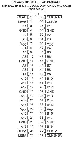 Specifications
Supply voltage range, VCC . . . . . . . . . . . . . . . . . . . . . . . . . . . . . . . . . . . . . . . . . . . . . . . . . . 0.5 V to 4.6 V
Input voltage range, VI (see Note 1) . . . . . . . . . . . . . . . . . . . . . . . . . . . . . . . . . . . . . . . . . . . 0.5 V to 7 V
Voltage range applied to any output in the high state or power-off state, VO (see Note 1) . .0.5 V to 7 V
Current into any output in the low state, IO : SN54LVT16501 . . . . . . . . . . . . . . . . . . . . . . . . . . . . . . . 96 mA
SN74LVT16501 . . . . . . . . . . . . . . . . . . . . . . . . . . . . ... 128 mA
Current into any output in the high state, IO (see Note 2): SN54LVT16501 . . . . . . . . . . . . . . . . . . .. . 48 mA
SN74LVT16501 . . . . . . . . . . . . . . . . . . . ...64 mA.
Input clamp current, IIK (VI < 0) . . . . . . . . . . . . . . . . . . . . . . . . . . . . . . . . . . . . . . . . . . . . . . . . . . . . 50 mA
Output clamp current, IOK (VO < 0) . . . . . . . . . . . . . . . . . . . . . . . . . . . . . . . . . . . . . . . . . . . . . . . . . 50 mA
Maximum power dissipation at TA = 55 (in still air) (see Note 3):DGG package . . . . . . . . . . . . . . . . ..... 1 W
DL package . . . . . . . . . . . . . . . ...... 1.4 W
Storage temperature range, Tstg . . . . . . . . . . . . . . . . . . . . . . . . . . . . . . . . . . . . . . . . . . . . . . .65 to 150
DescriptionThe SN74ALVTH16601 devices are 18-bit universal bus transceivers designed for 2.5-V or 3.3-V VCC operation, but with the capability to provide a TTL interface to a 5-V system environment. The SN74ALVTH16601 devices combine D-type latches and D-type flip-flops to allow data flow in transparent, latched, and clocked modes.
Data flow in each direction is controlled by output-enable (OEAB and OEBA), latch-enable (LEAB and LEBA), and clock (CLKAB and CLKBA) inputs. The clock can be controlled by the clock-enable (CLKENAB and CLKENBA) inputs. For A-to-B data flow, the device operates in the transparent mode when LEAB is high. When LEAB is low, the A data is latched if CLKAB is held at a high or low logic level. If LEAB is low, the A data is stored in the latch/flip-flop on the low-to-high transition of CLKAB. Output enable OEAB is active low. When OEAB is low, the outputs are active. When OEAB is high, the outputs are in the high-impedance state. Data flow for B to A is similar to that of A to B, but uses OEBA , LEBA, CLKBA, and CLKENBA.This SN74ALVTH16601 device is fully specified for hot-insertion applications using Ioff and power-up 3-state. The Ioff circuitry disables the outputs, preventing damaging current backflow through the device when it is powered down. The power-up 3-state circuitry places the outputs in the high-impedance state during power up and power down, which prevents driver conflict.
When VCC is between 0 and 1.2 V, the device is in the high-impedance state during power up or power down. However, to ensure the high-impedance state above 1.2 V,OE should be tied to V CC through a pullup resistor; the minimum value of the resistor is determined by the current-sinking capability of the driver. Active bus-hold circuitry is provided to hold unused or floating data inputs at a valid logic level.The SN54ALVTH16601 is characterized for operation over the full military temperature range of 55to 125. The SN74ALVTH16601 is characterized for operation from 40to 85.

 SN74ALVTH16601 Data Sheet


