Features: `State-of-the-Art Advanced BiCMOS Technology (ABT) Widebus™Design for 2.5-V and 3.3-V Operation and Low Static Power Dissipation
`Support Mixed-Mode Signal Operation (5-V Input and Output Voltages With 2.3-V to 3.6-V VCC)
`Typical VOLP (Output Ground Bounce) <0.8 V at VCC = 3.3 V, TA = 25°C
`High Drive (24/24 mA at 2.5-V VCC and 32/64 mA at 3.3-V VCC)
`LOFFand Power-Up 3-State Support Hot Insertion
`Use Bus Hold on Data Inputs in Place of External Pullup/Pulldown Resistors to Prevent the Bus From Floating
`Auto3-State Eliminates Bus Current Loading When Output Exceeds VCC + 0.5 V
`Flow-Through Architecture Facilitates Printed Circuit Board Layout
`Distributed VCC and GND Pin Configuration Minimizes High-Speed Switching Noise
`ESD Protection Exceeds JESD-22
2000-V Human-Body Model (A114-A)
200-V Machine Model (A115-A)
1000-V Charged-Device Model (C101)
`Latch-Up Performance Exceeds 100 mA Per JESD 78, Class II
`Packaged in Plastic Fine-Pitch Ball Grid Array Package
NOTE: For tape and reel order entry:
The GKER package is abbreviated to KR.
Pinout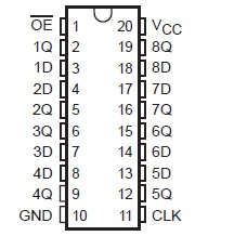 Specifications
Supply voltage range, VCC . . . . . . . . . . . . . . . . . . . . . . . . . . . . . . . . . . . . . . . . . 0.5 V to 4.6 V
Input voltage range, VI (see Note 1) . . . . . . . . . . . . . . . . . . . . . . . . . . . . . . . . . . . 0.5 V to 7 V
Voltage range applied to any output in the high-impedance
or power-off state, VO (see Note 1) . . . . . . . . . . . . . . . . . . . . . . . . . . . .. . . . . . . . . 0.5 V to 7 V
Voltage range applied to any output in the high state, VO (see Note 1) . . . . . . . . . 0.5 V to 7 V
Current into any output in the low state, IO: SN54ALVTH32244 . . . . . . . . .. . . . . . . . . . . . . 96 mA
SN74ALVTH32244 . . . . . . . . . . . . . . . . . . . . 128 mA
Current into any output in the high state, IO (see Note 2): SN54ALVTH32244 . . . . . . . . . . . 48 mA
SN74ALVTH32244 . . . . . . . . . . 64 mA
Input clamp current, IIK (VI < 0) . . . . . . . . . . . . . . . . . . . . . . . . . . . . . . . . . . . . . . . . . . . . . 50 mA
Output clamp current, IOK (VO < 0) . . . . . . . . . . . . . . . . . . . . . . . . . . . . . . . . . . . . . . . . . . . 50 mA
Package thermal impedance, JA (see Note 3) . . . . . . . . . . . . . . . . . . . . . . . . . . . . . . . . . 40°C/W
Storage temperature range, Tstg . . . . . . . . . . . . . . . . . . . . . . . . . . . . . . . . . . .. . 65°C to 150°C
† Stresses beyond those listed under "absolute maximum ratings" may cause permanent damage to the device. These are stress ratings only, and functional operation of the device at these or any other conditions beyond those indicated under "recommended operating conditions" is not implied. Exposure to absolute-maximum-rated conditions for extended periods may affect device reliability. NOTES: 1. The input and output negative-voltage ratings may be exceeded if the input and output clamp-current ratings are observed. 2. This current flows only when the output is in the high state and VO > V CC. 3. The package thermal impedance is calculated in accordance with JESD 51.
DescriptionThe SN74ALVTH32244 devices are 32-bit buffers/line drivers designed for 2.5-V or 3.3-V VCC operation, but with the capability to provide a TTL interface to a 5-V system environment. These SN74ALVTH32244 devices can be used as eight 4-bit buffers, four 8-bit buffers, two 16-bit buffers, or one 32-bit buffer. These devices provide true outputs and symmetrical active-low output-enable (OE) inputs.
When VCC is between 0 and 1.2-V, the devices are in the high-impedance state during power up or power down. However, to ensure the high-impedance state above 1.2-V, OE should be tied to VCC through a pullup resistor; the minimum value of the resistor is determined by the current-sinking capability of the driver. These SN74ALVTH32244 devices are fully specified for hot-insertion applications using Ioff and power-up 3-state. The Ioff circuitry disables the outputs, preventing damaging current backflow through the devices when they are powered down. The power-up 3-state circuitry places the outputs in the high-impedance state during power up and power down, which prevents driver conflict.
Active bus-hold circuitry is provided to hold unused or floating data inputs at a valid logic level.The SN54ALVTH32244 is characterized for operation over the full military temperature range of 55°C to 125°C. The SN74ALVTH32244 is characterized for operation from 40°C to 85°C.

 SN74ALVTH32244 Data Sheet


