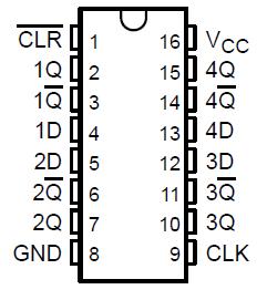
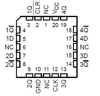
SN74AS175B: Application· Buffer/Storage Registers· Shift Registers· Pattern GeneratorsPinout SpecificationsSupply voltage, VCC . . . . . . . . . . . . . . . . . . . . . . . . . . . . . . . . . . . . . . . . . ....
floor Price/Ceiling Price
- Part Number:
- SN74AS175B
- Supply Ability:
- 5000
Price Break
- Qty
- 1~5000
- Unit Price
- Negotiable
- Processing time
- 15 Days
SeekIC Buyer Protection PLUS - newly updated for 2013!
- Escrow Protection.
- Guaranteed refunds.
- Secure payments.
- Learn more >>
Month Sales
268 Transactions
Payment Methods
All payment methods are secure and covered by SeekIC Buyer Protection PLUS.

 SN74AS175B Data Sheet


