SeekIC No. : 004498380
Detail
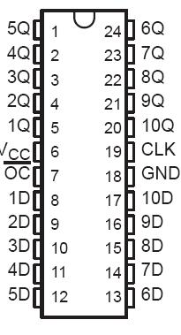
SN74AS1821: Features: • Center VCC and GND Configuration Provides Minimum Lead Inductance in High Current Switching Applications• Provides Extra Data Width Necessary for Wider Address/Data Paths or ...
 SN74AS1821 Data Sheet
floor Price/Ceiling Price
- Part Number:
- SN74AS1821
- Supply Ability:
- 5000
Price Break
- Qty
- 1~5000
- Unit Price
- Negotiable
- Processing time
- 15 Days
SeekIC Buyer Protection PLUS - newly updated for 2013!
- Escrow Protection.
- Guaranteed refunds.
- Secure payments.
- Learn more >>
Month Sales
268 Transactions
Payment Methods
All payment methods are secure and covered by SeekIC Buyer Protection PLUS.
Notice: When you place an order, your payment is made to SeekIC and not to your seller. SeekIC only pays the seller after confirming you have received your order. We will also never share your payment details with your seller.