Features: ` Optimized for 1.8-V Operation and is 3.6-V I/O Tolerant to Support Mixed-Mode Signal Operation
` Ioff Supports Partial-Power-Down Mode Operation
` Sub 1-V Operable
` Max tpd of 1.7 ns at 1.8 V
` Low Power Consumption, 20-A Max ICC
` ±8-mA Output Drive at 1.8 V
` Latch-Up Performance Exceeds 100 mA Per JESD 78, Class II
` ESD Protection Exceeds JESD 22
2000-V Human-Body Model (A114-A)
200-V Machine Model (A115-A)
1000-V Charged-Device Model (C101)
Pinout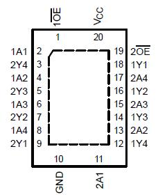 Specifications
Supply voltage range, VCC . . . . . . . . . . . . . . . . . . . . . . . . . . . . . . . . . . . . . . 0.5 V to 3.6 V
Input voltage range, VI (see Note 1) . . . . . . . . . . . . . . . . . . . . . . . . . . .. . . . 0.5 V to 3.6 V
Voltage range applied to any output in the high-impedance or power-off state, VO
(see Note 1) . . . . . . . . . . . . . . . . . . . . . . . . . . . . . . . . . . . . . . . . . . . . . . .. . . 0.5 V to 3.6 V
Output voltage range, VO (see Note 1) . . . . . . . . . . . . . . . .. . . . . . . . 0.5 V to VCC + 0.5 V
Input clamp current, IIK (VI < 0) . . . . . . . . . . . . . . . . . . . . . . . . . . . . . . . . . . . .. . . . . 50 mA
Output clamp current, IOK (VO < 0) . . . . . . . . . . . . . . . . . . . . . . . . . . . . . . . . . . . . . . 50 mA
Continuous output current, IO . . . . . . . . . . . . . . . . . . . . . . . . . . . . . . . . . . . . . . . . . . ±20 mA
Continuous current through VCC or GND . . . . . . . . . . . . . . . . . . . . . . . . . . . . . . . . . ±100 mA
Package thermal impedance, JA (see Note 2) . . . . . . . . . . . . . . . . . . . . . . . . . . . . . 37°C/W
Storage temperature range, Tstg . . . . . . . . . . . . . . . . . . . . . . . . . . . . . . . . 65°C to 150°C
† Stresses beyond those listed under "absolute maximum ratings" may cause permanent damage to the device. These are stress ratings only, and functional operation of the device at these or any other conditions beyond those indicated under "recommended operating conditions" is not implied. Exposure to absolute-maximum-rated conditions for extended periods may affect device reliability.
NOTES: 1. The input negative-voltage and output voltage ratings may be exceeded if the input and output current ratings are observed.
2. The package thermal impedance is calculated in accordance with JESD 51-5.
DescriptionThis SN74AUC240 octal buffer/driver is operational at 0.8-V to 2.7-V VCC, but is designed specifically for 1.65-V to 1.95-V VCC operation.
The SN74AUC240 is designed specifically to improve the performance and density of 3-state memory address drivers, clock drivers, and bus-oriented receivers and transmitters.
This SN74AUC240 device is organized as two 4-bit buffers/drivers with separate output-enable (OE) inputs. When OE is low, the device passes data from the A inputs to the Y outputs. When OE is high, the outputs are in the
high-impedance state.
To ensure the SN74AUC240 high-impedance state during power up or power down, OE should be tied to VCC through a pullup resistor; the minimum value of the resistor is determined by the current-sinking capability of the driver.
This SN74AUC240 device is fully specified for partial-power-down applications using Ioff. The Ioff circuitry disables the outputs,
preventing damaging current backflow through the device when it is powered down.

 SN74AUC240 Data Sheet


