Features: ` Available in the Texas Instruments NanoStar and NanoFree Packages
` Optimized for 1.8-V Operation and Is 3.6-V I/O Tolerant to Support Mixed-Mode Signal Operation
` Ioff Supports Partial-Power-Down Mode Operation
` Sub 1-V Operable
` Max tpd of 1.5 ns at 1.8 V
` Low Power Consumption, 10 A at 1.8 V
` ±8-mA Output Drive at 1.8 V
` Latch-Up Performance Exceeds 100 mA Per JESD 78, Class II
` ESD Protection Exceeds JESD 22 − 2000-V Human-Body Model (A114-A) − 200-V Machine Model (A115-A) − 1000-V Charged-Device Model (C101)Pinout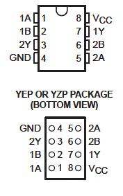 Specifications
Supply voltage range, VCC . . . . . . . . . . . . . . . . . . . . . . . . . . . . . . . . . . . . . . . . . . . . . . . . . . . . . . . . . −0.5 V to 3.6 V
Input voltage range, VI (see Note 1) . . . . . . . . . . . . . . . . . . . . . . . . . . . . . . . . . . . . . . . . . . . . . . . . . −0.5 V to 3.6 V
Voltage range applied to any output in the high-impedance or power-off state, VO
(see Note 1) . . . . . . . . . . . . . . . . . . . . . . . . . . . . . . . . . . . . . . . . . . . . . . . . . . . . . . . . . . . . . . . . . . . −0.5 V to 3.6 V
Output voltage range, VO (see Note 1) . . . . . . . . . . . . . . . . . . . . . . . . . . . . . . . . . . . . . . . . −0.5 V to VCC + 0.5 V
Input clamp current, IIK (VI < 0) . . . . . . . . . . . . . . . . . . . . . . . . . . . . . . . . . . . . . . . . . . . . . . . . . . . . . . . . . . . −50 mA
Output clamp current, IOK (VO < 0) . . . . . . . . . . . . . . . . . . . . . . . . . . . . . . . . . . . . . . . . . . . . . . . . . . . . . . . . −50 mA
Continuous output current, IO . . . . . . . . . . . . . . . . . . . . . . . . . . . . . . . . . . . . . . . . . . . . . . . . . . . . . . . . . . . . . ±20 mA
Continuous current through VCC or GND . . . . . . . . . . . . . . . . . . . . . . . . . . . . . . . . . . . . . . . . . . . . . . . . . . ±100 mA
Package thermal impedance, JA (see Note 2): DCT package . . . . . . . . . . . . . . . . . . . . . . . . . . . . . . . 220°C/W
DCU package . . . . . . . . . . . . . . . . . . . . . . . . . . . . . . . 227°C/W
YEP/YZP package . . . . . . . . . . . . . . . . . . . . . . . . . . . 102°C/W
Storage temperature range, Tstg . . . . . . . . . . . . . . . . . . . . . . . . . . . . . . . . . . . . . . . . . . . . . . . . . . . −65°C to 150°C
† Stresses beyond those listed under "absolute maximum ratings" may cause permanent damage to the device. These are stress ratings only, and functional operation of the device at these or any other conditions beyond those indicated under "recommended operating conditions" is not implied. Exposure to absolute-maximum-rated conditions for extended periods may affect device reliability.
NOTES:
1. The input negative-voltage and output voltage ratings may be exceeded if the input and output current ratings are observed.
2. The package thermal impedance is calculated in accordance with JESD 51-7.
DescriptionThis SN74AUC2G08 dual 2-input positive-AND gate is operational at 0.8-V to 2.7-V VCC, but is designed specifically for 1.65-V to 1.95-V VCC operation.
The SN74AUC2G08 performs the Boolean function Y � A • B or Y � A�B in positive logic.
SN74AUC2G08 NanoStar and NanoFree package technology is a major breakthrough in IC packaging concepts, using the die as the package.
This SN74AUC2G08 device is fully specified for partial-power-down applications using Ioff. The Ioff circuitry disables the outputs, preventing damaging current backflow through the device when it is powered down.
For more SN74AUC2G08 information about AUC Little Logic devices, please refer to the TI application report, Applications of Texas Instruments AUC Sub-1-V Little Logic Devices, literature number SCEA027.

 SN74AUC2G08 Data Sheet


