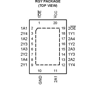
Pinout

 SpecificationsSupply voltage range, V CC . . . . . . . . . . . . . . . . . . . . 0.5 V to 3.6 V
Input voltage range, V I (see Note 1) . . . . . . . . . . . . 0.5 V to 3.6 V
Voltage range applied to any output in the high-impedance or power-off state, V O
(see Note 1) . . . . . . . . . . . . . . . . . . . . . . . . . . . . . . . . . . . . .. . 0.5 V to 3.6 V
Output voltage range, V O (see Note 1) . . . . . . . . . . . . 0.5 V to V CC+ 0.5 V
Input clamp current, I IK (V I < 0) . . . . . . . . . . . . . . . . . . . . . . . . . . . 50 mA
Output clamp current, I OK (V O < 0) . . . . . . . . . . . . . . . . . . . . . . . . . . 50 mA
Continuous output current, I O . . . . . . . . . . . . . . . . . . . . . . . . . . . . . . ±20 mA
Continuous current through V CC or GND . . . . . . . . . . . . . . . . . . . . . . ±100 mA
Package thermal impedance, JA (see Note 2): . . . . . . . . . . . . . . . . .. . . 37°C/W
Storage temperature range, T stg . . . . . . . . . . . . . . . . . . . . . . . 65 to 150
DescriptionThis SN74AUCH244 octal buffer/driver is operational at 0.8-V to 2.7-V V CC , but is designed specifically for 1.65-V to 1.95-V V CC operation.
The SN74AUCH244 is organized as two 4-bit line drivers with separate output-enable (OE) inputs. When OE is low, the device passes data from the A inputs to the Y outputs. When OE is high, the outputs are in the high-impedance state.
To ensure the SN74AUCH244 high-impedance state during power up or power down, OE should be tied to V CC through a pullup resistor; the minimum value of the resistor is determined by the current-sinking capability of the driver.
SN74AUCH244 Active bus-hold circuitry holds unused or undriven inputs at a valid logic state. Use of pullup or pulldown resistors with the bus-hold circuitry is not recommended.
This SN74AUCH244 device is fully specified for partial-power-down applications using I . The I circuitry disables the outputs, off off preventing damaging current backflow through the device when it is powered down.

 SN74AUCH244 Data Sheet


