Minimum Operating Temperature
:
Operating Temperature Range
:
Packaging
: Reel
Maximum Operating Temperature
: + 85 C
Logic Type
: CMOS
Number of Circuits
: 1
High Level Output Current
: - 4 mA
Low Level Output Current
: 4 mA
Supply Voltage - Max
: 3.6 V
Package / Case
: SOT-23-5
Supply Voltage - Min
: 0.8 V
Logic Family
: AUP
Propagation Delay Time
: 17.1 ns, 12.3 ns, 10.3 ns, 7.4 ns, 6.2 ns
Features: ` Available in the Texas Instruments
NanoStar and NanoFree Packages
` Low Static-Power Consumption;
ICC = 0.9-A Max
` Low Dynamic-Power Consumption;
Cpd = 4.4 pF Typical at 3.3 V
` Low Input Capacitance; Ci = 1.5 pF Typical
` Low Noise − Overshoot and Undershoot <10% of VCC
` Ioff Supports Partial-Power-Down Mode Operation
` Includes Schmitt-Trigger Inputs
` Wide Operating VCC Range of 0.8 V to 3.6 V
` Optimized for 3.3-V Operation
` 3.6-V I/O Tolerant to Support Mixed-Mode
Signal Operation
` tpd = 4.9 ns Max at 3.3 V
` Suitable for Point-to-Point Applications
` Latch-Up Performance Exceeds 100 mA Per
JESD 78, Class II
` ESD Performance Tested Per JESD 22
− 2000-V Human-Body Model
(A114-B, Class II)
− 200-V Machine Model (A115-A)
− 1000-V Charged-Device Model (C101)
` ESD Protection Exceeds ±5000-V With
Human-Body ModelPinout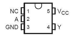 SpecificationsSupply voltage range, VCC . . . . . . . . . . . . . . . . . . . . . . . . . . . . . . . . . . . . . . . . . . . . . . . . . . .−0.5 V to 4.6 V
Input voltage range, VI (see Note 1) . . . . . . . . . . . . . . . . . . . . . . . . . . . . . . . . . . . . . . . . . . −0.5 V to 4.6 V
Voltage range applied to any output in the high-impedance or power-off state, VO
(see Note 1) . . . . . . . . . . . . . . . . . . . . . . . . . . . . . . . . . . . . . . . . . . . . . . . . . . . . . . . . . . . . . . −0.5 V to 4.6 V
Output voltage range in the high or low state, VO (see Note 1) . . . . . . . . . . . . . . . . . −0.5 V to VCC + 0.5 V
Input clamp current, IIK (VI < 0) . . . . . . . . . . . . . . . . . . . . . . . . . . . . . . . . . . . . . . . . . . . . . . . . . . . . −50 mA
Output clamp current, IOK (VO < 0) . . . . . . . . . . . . . . . . . . . . . . . . . . . . . . . . . . . . . . . . . . . . . . . . . . −50 mA
Continuous output current, IO . . . . . . . . . . . . . . . . . . . . . . . . . . . . . . . . . . . . . . . . . . . . . . . . . . . . . . ±20 mA
Continuous current through VCC or GND . . . . . . . . . . . . . . . . . . . . . . . . . . . . . . . . . . . . . . . . . . . . . . . ±50 mA
Package thermal impedance, JA (see Note 2): DBV package . . . . . . . . . . . . . . . . . . . . . . . . . . . . . .206°C/W
DCK package . . . . . . . . . . . . . . . . . . . . . . . . . . . . . . . . . . . . . . . . . . . . . . . . . . . . . . . . . . . . . . . . . . 252°C/W
YEP/YZP package . . . . . . . . . . . . . . . . . . . . . . . . . . . . . . . . . . . . . . . . . . . . . . . . . . . . . . . . . . . . . . . 132°C/W
Storage temperature range, Tstg . . . . . . . . . . . . . . . . . . . . . . . . . . . . . . . . . . . . . . . . . . . . . .−65°C to 150°C
† Stresses beyond those listed under "absolute maximum ratings" may cause permanent damage to the device. These are stress ratings only, and
functional operation of the device at these or any other conditions beyond those indicated under "recommended operating conditions" is not
implied. Exposure to absolute-maximum-rated conditions for extended periods may affect device reliability.
NOTES: 1. The input and outpu negative-voltaget ratings may be exceeded if the input and output current ratings are observed.
2. The package thermal impedance is calculated in accordance with JESD 51-7.DescriptionThe AUP family is TI's premier solution to the industry's low-power needs in battery-powered portable applications. This SN74AUP1G14DBVR family ensures a very low static and dynamic power consumption across the entire VCC range of 0.8 V to 3.6 V, resulting in an increased battery life. This SN74AUP1G14DBVR product also maintains excellent signal integrity (see Figures 1 and 2).
This SN74AUP1G14DBVR device functions as an independent gate with Schmitt-trigger inputs, which allows for slow input transition and better switching-noise immunity at the input.
SN74AUP1G14DBVR NanoStar and NanoFree package technology is a major breakthrough in IC packaging concepts, using the die as the package.
Parameters: | Technical/Catalog Information | SN74AUP1G14DBVR |
| Vendor | Texas Instruments (VA) |
| Category | Integrated Circuits (ICs) |
| Number of Circuits | 1 - Single |
| Package / Case | SOT-23-5 |
| Logic Type | Inverter with Schmitt Trigger |
| Packaging | Digi-Reel? |
| Mounting Type | Surface Mount |
| Number of Inputs | 1 |
| Current - Output High, Low | 4mA, 4mA |
| Supply Voltage | 0.8 V ~ 3.6 V |
| Operating Temperature | -40°C ~ 85°C |
| Voltage - Supply | 0.8 V ~ 3.6 V |
| Drawing Number | 296; 4073253-4; DBV; 5 |
| Lead Free Status | Lead Free |
| RoHS Status | RoHS Compliant |
| Other Names | SN74AUP1G14DBVR
SN74AUP1G14DBVR
296 18213 6 ND
296182136ND
296-18213-6
|

 SN74AUP1G14DBVR Data Sheet


