Features: ` Member of the Texas Instruments
WidebusE Family
` EPICE (Enhanced-Performance Implanted
CMOS) Submicron Process
` DOCE (Dynamic Output Control) Circuit
Dynamically Changes Output Impedance,
Resulting in Noise Reduction Without
Speed Degradation
` Dynamic Drive Capability Is Equivalent to
Standard Outputs With IOH and IOL of
±24 mA at 2.5-V VCC
` Overvoltage-Tolerant Inputs/Outputs Allow
Mixed-Voltage-Mode Data Communications
` Ioff Supports Partial-Power-Down Mode Operation
` ESD Protection Exceeds JESD 22
2000-V Human-Body Model (A114-A)
200-V Machine Model (A115-A)
` Latch-Up Performance Exceeds 100 mA Per
JESD 78, Class II
` Package Options Include Plastic Thin
Shrink Small-Outline (DGG) and Thin Very
Small-Outline (DGV) PackagesPinout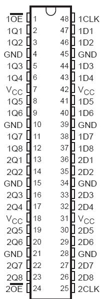 SpecificationsSupply voltage range, VCC . . . . . . . . . . . . . . . . . . . . . . . . . . . . . . . . . . . . . . . . . . . . . . . . .0.5 V to 4.6 V
Input voltage range, VI (see Note 1) . . . . . . . . . . . . . . . . . . . . . . . . . . . . . . . . . . . . . . . . .0.5 V to 4.6 V
Voltage range applied to any output in the high-impedance or power-off state, VO
(see Note 1) . . . . . . . . . . . . . . . . . . . . . . . . . . . . . . . . . . . . . . . . . . . . . . . . . . . . . . . . . . . .0.5 V to 4.6 V
Voltage range applied to any output in the high or low state, VO
(see Notes 1 and 2) . . . . . . . . . . . . . . . . . . . . . . . . . . . . . . . . . . . . . . . . . . . . . . . . .0.5 V to VCC + 0.5 V
Input clamp current, IIK (VI < 0) . . . . . . . . . . . . . . . . . . . . . . . . . . . . . . . . . . . . . . . . . . . . . . . . . . .50 mA
Output clamp current, IOK (VO < 0) . . . . . . . . . . . . . . . . . . . . . . . . . . . . . . . . . . . . . . . . . . . . . . . . .50 mA
Continuous output current, IO . . . . . . . . . . . . . . . . . . . . . . . . . . . . . . . . . . . . . . . . . . . . . . . . . . . . .±50 mA
Continuous current through each VCC or GND . . . . . . . . . . . . . . . . . . . . . . . . . . . . . . . . . . . . . . . . ±100 mA
Package thermal impedance, qJA (see Note 3): DGG package . . . . . . . . . . . . . . . . . . . . . . . . . . . . .70°C/W
DGV package . . . . . . . . . . . . . . . . . . . . . . . . . . . . . . . . . . . . . . . . . . . . . . . . . . . . . . . . . . . . . . . . . .58°C/W
Storage temperature range, Tstg . . . . . . . . . . . . . . . . . . . . . . . . . . . . . . . . . . . . . . . . . . . .65°C to 150°C
† Stresses beyond those listed under "absolute maximum ratings" may cause permanent damage to the device. These are stress ratings only, and
functional operation of the device at these or any other conditions beyond those indicated under "recommended operating conditions" is not
implied. Exposure to absolute-maximum-rated conditions for extended periods may affect device reliability.
NOTES: 1. The input and output negative-voltage ratings may be exceeded if the input and output current ratings are observed.
2. The output positive-voltage rating may be exceeded up to 4.6 V maximum if the output current rating is observed.
3. The package thermal impedance is calculated in accordance with JESD 51.DescriptionA SN74AVC16374DGG Dynamic Output Control (DOC) circuit is implemented, which, during the transition, initially lowers the output impedance to effectively drive the load and, subsequently, raises the impedance to reduce noise. Figure 1 shows typical VOL vs IOL and VOH vs IOH curves to illustrate the output impedance and drive capability of the circuit. At the beginning of the signal transition, the DOC circuit provides a maximum dynamic drive that is equivalent to a high-drive standard-output device. For more information, refer to the TI application reports, AVC Logic Family Technology and Applications, literature number SCEA006, and Dynamic Output Control (DOCE) Circuitry Technology and Applications, literature number SCEA009.
The SN74AVC16374 is particularly suitable for implementing buffer registers, I/O ports, bidirectional bus drivers, and working registers. It can be used as two 8-bit flip-flops or one 16-bit flip-flop. On the positive transition of the clock (CLK) input, the Q outputs of the flip-flop take on the logic levels at the data (D) inputs. OE can be used to place the eight outputs in either a normal logic state (high or low logic levels) or the high-impedance state. In the high-impedance state, the outputs neither load nor drive the bus lines significantly. The high-impedance state and the increased drive provide the capability to drive bus lines without need for interface or pullup components.
SN74AVC16374DGG OE does not affect internal operations of the flip-flop. Old data can be retained or new data can be entered while the outputs are in the high-impedance state.
To ensure the SN74AVC16374DGG high-impedance state during power up or power down, OE should be tied to VCC through a pullupresistor; the minimum value of the resistor is determined by the current-sinking capability of the driver. This device is fully specified for partial-power-down applications using Ioff. The Ioff circuitry disables the outputs, preventing damaging current backflow through the device when it is powered down. The SN74AVC16374 is characterized for operation from 40°C to 85°C.

 SN74AVC16374DGG Data Sheet


