Pinout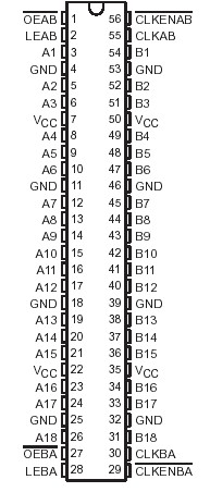 SpecificationsSupply voltage range, VCC . . . . . . . . . . . . . . . . . . . . . . . . . . . . . . . . . . . . . . . . . . . . . . .0.5 V to 4.6 V
Input voltage range, VI (see Note 1) . . . . . . . . . . . . . . . . . . . . . . . . . . . . . . . . . . . . . . . .0.5 V to 4.6 V
Voltage range applied to any input/output when the output
is in the high-impedance or power-off state, VO (see Note 1) . . . . . . . . . . . . . . . . . . 0.5 V to 4.6 V
Voltage range applied to any input/output when the output
is in the high or low state, VO (see Notes 1 and 2) . . . . . . . . . . . . . . . . . . . . . . .0.5 V to VCC + 0.5 V
Input clamp current, IIK (VI < 0) . . . . . . . . . . . . . . . . . . . . . . . . . . . . . . . . . . . . . . . . . . . . . . . . . .50 mA
Output clamp current, IOK (VO < 0) . . . . . . . . . . . . . . . . . . . . . . . . . . . . . . . . . . . . . . . . . . . . . . . .50 mA
Continuous output current, IO . . . . . . . . . . . . . . . . . . . . . . . . . . . . . . . . . . . . . . . . . . . .. . . . . . . .±50 mA
Continuous current through each VCC or GND . . . . . . . . . . . . . . . . . . . . . . . . . .. . . . . . . . . . . . .±100 mA
Package thermal impedance, JA (see Note 3): DGG package . . . . . . . . . . . . . . . . . . . . . . . .. . . .64°C/W
DGV package . . . . . . . . . . . . . . . . . . . . .. . . . . . .48°C/W
Storage temperature range, Tstg . . . . . . . . . . . . . . . . . . . . . . . . . . . . . . . . . . . . . . .. . . . .65°C to 150°C DescriptionA SN74AVC16601 Dynamic Output Control (DOC) circuit is implemented, which, during the transition, initially lowers the output impedance to effectively drive the load and, subsequently, raises the impedance to reduce noise. Figure 1 shows typical VOL vs IOL and VOH vs IOH curves to illustrate the output impedance and drive capability of the circuit. At the beginning of the signal transition, the DOC circuit provides a maximum dynamic drive that is equivalent to a high-drive standard-output device. For more information, refer to the TI application reports, AVC Logic Family Technology and Applications, literature number SCEA006, and Dynamic Output Control (DOCE) Circuitry Technology and Applications, literature number SCEA009.
This SN74AVC16601 18-bit edge-triggered D-type flip-flop is operational at 1.2-V to 3.6-V VCC, but is designed specifically for 1.65-V to 3.6-V VCC operation.
SN74AVC16601 Data flow in each direction is controlled by output-enable (OEAB and OEBA), latch-enable (LEAB and LEBA), and clock (CLKAB and CLKBA) inputs. The clock can be controlled by the clock-enable (CLKENAB and CLKENBA) inputs. For A-to-B data flow, the device operates in the transparent mode when LEAB is high. When LEAB is low, the A data is latched if CLKAB is held at a high or low logic level. If LEAB is low, the A data is stored in the latch/flip-flop on the low-to-high transition of CLKAB. Output enable OEAB is active low. When OEAB is low, the outputs are active. When OEAB is high, the outputs are in the high-impedance state.
SN74AVC16601 Data flow for B to A is similar to that of A to B, but uses OEBA, LEBA, and CLKBA.
To ensure the SN74AVC16601 high-impedance state during power up or power down, OE should be tied to VCC through a pullup resistor; the minimum value of the resistor is determined by the current-sinking capability of the driver.
This SN74AVC16601 device is fully specified for partial-power-down applications using Ioff. The Ioff circuitry disables the outputs, preventing damaging current backflow through the device when it is powered down.
The SN74AVC16501 is characterized for operation from 40°C to 85°C.

 SN74AVC16601 Data Sheet


