Features: Control Inputs VIH/VIL Levels are Referenced to VCCA Voltage
VCC Isolation Feature − If Either VCC Input Is at GND, Both Ports Are in the High-Impedance State
Overvoltage-Tolerant Inputs/Outputs Allow Mixed-Voltage-Mode Data Communications
Fully Configurable Dual-Rail Design Allows Each Port to Operate Over the Full 1.2-V to 3.6-V Power-Supply Range
Ioff Supports Partial-Power-Down Mode Operation
I/Os Are 4.6-V Tolerant
Max Data Rates
− 380 Mbps (1.8-V to 3.3-V Translation)
− 260 Mbps (< 1.8-V to 3.3-V Translation)
− 260 Mbps (Translate to 2.5 V)
− 210 Mbps (Translate to 1.8 V)
− 120 Mbps (Translate to 1.5 V)
− 100 Mbps (Translate to 1.2 V)
Latch-Up Performance Exceeds 100 mA Per JESD 78, Class II
ESD Protection Exceeds JESD 22
− 8000-V Human-Body Model (A114-A)
− 200-V Machine Model (A115-A)
− 1000-V Charged-Device Model (C101)Pinout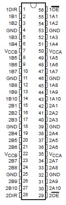 Specifications
Supply voltage range, VCCA and VCCB . . . . . . . . . . . . . . . ... . . . . . . . . −0.5 V to 4.6 V
Input voltage range, VI (see Note 1): I/O ports (A port) . . . . . . . . . . . −0.5 V to 4.6 V
I/O ports (B port) . . . .. . . . . . . . −0.5 V to 4.6 V
Control inputs . . . . . . . . . . . . . . −0.5 V to 4.6 V
Voltage range applied to any output in the high-impedance or power-off state, VO
(see Note 1): (A port) . . . . . . . . . . . . . . . . .. . . . . . . . . . . . . . . . . . . . . . −0.5 V to 4.6 V
(B port) . . . . . . . . . . . . . . . . . . . . . . . . . . . . . . . . . . . . . . −0.5 V to 4.6 V
Voltage range applied to any output in the high or low state, VO
(see Notes 1 and 2): (A port) . . . . . . . . . . . . . . . . . . .... . . . . . . −0.5 V to VCCA + 0.5 V
(B port) . . . . . . . . . . . . . . . . . . . . . . . .. . . −0.5 V to VCCB + 0.5 V
Input clamp current, IIK (VI < 0) . . . . . . . . . . . . . . . . . . . . . . . . . . . . . . . . . . . . −50 mA
Output clamp current, IOK (VO < 0) . . . . . . . . . . . . . . . .. . . . . . . . . . . . . . . . . . . −50 mA
Continuous output current, IO . . . . . . . . . . . . . . . . . . . . . . . . . . . . . . . . . . . . . . ±50 mA
Continuous current through each VCCA, VCCB, and GND . . . . . . . . . . . .. . . . . . ±100 mA
Package thermal impedance, JA (see Note 3): DGG package . . . . . . . . . . . . . . 64°C/W
DGV package . . . . . . . . . . . . . . 48°C/W
GQL/ZQL package . . . . . . . . . . . 42°C/W
Storage temperature range, Tstg . . . . . . . . . . . . . . . . . .. . . . . . . . . . . . −65°C to 150°C
† Stresses beyond those listed under "absolute maximum ratings" may cause permanent damage to the device.These are stress ratings only, and functional operation of the device at these or any other conditions beyond those indicated under "recommended operating conditions" is not implied. Exposure to absolute-maximum-rated conditions for extended periods may affect device reliability.
NOTES: 1. The input voltage and output negative-voltage ratings may be exceeded if the input and output current ratings are observed.
2. The output positive-voltage rating may be exceeded up to 4.6 V maximum if the output current rating is observed.
3. The package thermal impedance is calculated in accordance with JESD 51-7.
DescriptionThis SN74AVC20T245 20-bit noninverting bus transceiver uses two separate configurable power-supply rails.
The SN74AVC20T245 is optimized to operate with VCCA/VCCB set at 1.4 V to 3.6 V. It is operational with VCCA/VCCB as low as 1.2 V. The A port is designed to track VCCA. VCCA accepts any supply voltage from 1.2 V to 3.6 V. The B port is designed to track VCCB. VCCB accepts any supply voltage from 1.2 V to 3.6 V. This allows for universal low-oltage bidirectional translation between any of the 1.2-V, 1.5-V, 1.8-V, 2.5-V, and 3.3-V voltage nodes.
The SN74AVC20T245 is designed for asynchronous communication between data buses. The device transmits data from the A bus to the B bus or from the B bus to the A bus, depending on the logic level at the direction-control (DIR) input. The output-enable (OE) input is used to disable the outputs so that the buses are isolated.
The SN74AVC20T245 is designed so that the control (1DIR, 2DIR, 1OE, and 2OE) inputs are supplied by VCCA.
This SN74AVC20T245 device is fully specified for partial-power-down applications using Ioff. The Ioff circuitry disables the outputs,preventing damaging current backflow through the device when it is powered down.
The VCC isolation feature ensures that if either VCC input is at GND, both ports are in the high-impedance state.
To ensure the SN74AVC20T245 high-impedance state during power up or power down, OE should be tied to VCC through a pullup resistor; the minimum value of the resistor is determined by the current-sinking capability of the driver.

 SN74AVC20T245 Data Sheet


